


UNIST Develops Ultra-Compact, Low-Power Clock Generation Circuit with Minimized Reference Spurs
 Published2026.02.12 13:16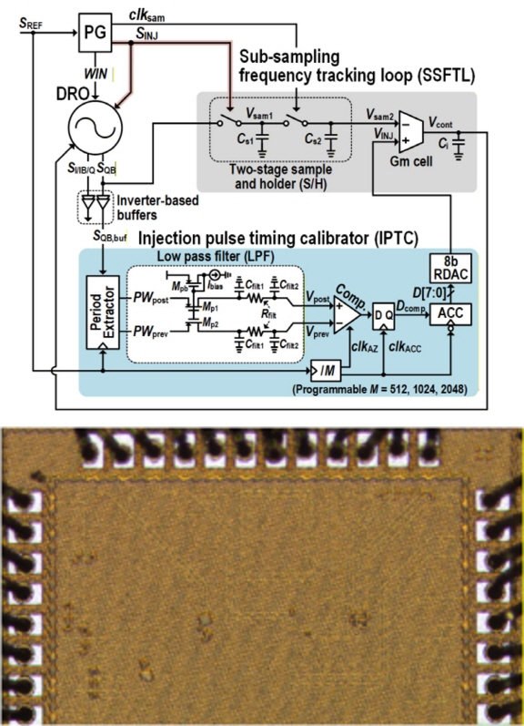
Recording -81.36 dBc at 2.1 GHz… Improved ring VCO-based ILCM performance, published in IEEE JSSC
An ultra-small, low-power circuit technology has been developed that minimizes reference spurs in clock signals, which determine the high-speed operation of semiconductor chips. The technology has been numerically demonstrated to deliver high-quality clock signals, a requirement for high-speed processing of large amounts of data, such as 5G and 6G communication chips and AI chips.
A research team led by Professor Hee-In Yoon of the Department of Electrical and Electronic Engineering at UNIST announced on the 11th that they have developed a semiconductor circuit for generating clock signals based on an ILCM (Injection-Locked Clock Multiplier) that significantly reduces noise. The results of the research were published in the February 6th issue of the IEEE Journal of Solid-State Circuits, an academic journal in the field of semiconductor circuits.
■ Application of reference spur suppression design
Semiconductor chips operate in response to a clock, a periodic electrical signal. In high-speed communications and AI computing environments, noise characteristics of the clock signal, such as jitter and reference spurs, directly impact system performance. Although the ILCM method is advantageous in reducing jitter, it has a limitation in that reference spurs occur during the reference signal injection process.
The research team adopted a ring oscillator (Ring VCO)-based ILCM structure and applied frequency tracking (SSFTL) and reference signal injection timing compensation (IPTC) designs to minimize reference spurs.
■ -81.36dBc at 2.1GHz·Jitter 280.9fs
The developed circuit achieved a reference spur of –81.36 dBc at 2.1 GHz output, the lowest level among reported ring oscillator-based ILCM circuits. Jitter was also reduced to 280.9 femtoseconds (fs).
Based on the 28nm CMOS process, the circuit area is 0.0444mm² and power consumption is 12.28mW, achieving both integration and power efficiency. The research team explained that the technology can be utilized in 6G communications, AI chips, and clock sources for high-speed interconnects.
This study was conducted with the support of the "Regional Intelligence Innovation Talent Development Project" from the Ministry of Science and ICT, the Semiconductor Design Education Center (IDEC), and the Institute for Information and Communications Technology Planning and Evaluation (IITP).

Comments
Related news

Intel Unveils Next-Generation 'Core Ultra Series 3' and vPro Platform for Enterprise PCs
Intel has officially unveiled the "Intel Core Ultra Series 3" for next-generation enterprise PCs and the latest vPro platform, addressing a wide range of demands from enterprise notebooks to high-performance workstations.
2026.03.26by 배종인 기자

ROHM Launches ESD Protection Diode Compatible with High-Speed Interfaces of 10Gbps or Higher
Semiconductor specialist ROHM has developed the 'RESDxVx series' of ESD (electrostatic discharge) protection diodes capable of responding to next-generation high-speed data communication environments exceeding 10Gbps, simultaneously enhancing both signal quality maintenance required in high-speed interfaces and IC protection performance.
2026.03.26by 배종인 기자

ST Launches 75V Drive IC Targeting 48V Industrial Motor Driving
ST Microelectronics has unveiled the 'STSPIN9P' series of 75V motor drive ICs tailored for 48V-class industrial drive system design. The new product family is characterized by half-bridge and full-bridge configurations that enable design scalability according to motor type and output conditions. Power supply circuits, protection functions, and current sensing circuits are integrated on-chip to simplify system configuration, and the devices are designed to support applications up to 500W maximum. The company plans to provide reference designs and demo boards to support development and evaluation in industrial automation, robotics, pumps, fans, lighting, and textile machinery.
2026.03.26by 배종인 기자

Nordic supports security updates for the entire lifecycle of IoT devices at a single fixed cost
Nordic Semiconductor, a global leader in low-power wireless connectivity solutions, has unveiled a single fixed-cost licensing model that delivers FOTA (Firmware Over-the-Air) and device management capabilities throughout the device lifecycle via nRF Cloud, and introduced a new firmware update solution to prepare for the enforcement of the European Union's Cyber Resilience Act (CRA).
2026.03.26by 배종인 기자

Practical Training in Low-Noise, Low-Power Circuit Design All in One Place… Training Fee Support
The "2026 Advanced Engineer Practical Masterclass" to strengthen competencies in high-sensitivity analog circuit and sensor-based system design will be held on April 16 at the e4ds Conference Center in Gasan-dong, Seoul. This program will be conducted as an offline paid hands-on training session, not online, and is targeted at engineers seeking on-site intensive learning. Texas Instruments will provide educational support for this training, allowing participation at 150,000 won, a 100,000 won discount from the original price of 250,000 won.
2026.03.26by 배종인 기자











