


Samsung Electronics enables communication with smart LED platform
 Published2016.03.15 09:31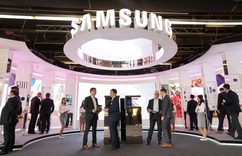
Wired and wireless communication information transmission based on an LED lighting platform
It is possible to analyze the presence of vehicles in large parking lots and shopper spending trends.
Samsung Electronics participated in the world's largest lighting and architecture exhibition, 'Light+Building 2016,' which has been held in Frankfurt, Germany since the 13th. Held every two years in Frankfurt, Germany, it is the world's largest exhibition in the field of lighting and architecture technology, with approximately 220,000 people from 161 countries around the world participating.
The new products unveiled by Samsung Electronics are a 'Smart Lighting Module' and an ultra-compact 'Chip Scale Package (CSP),' which enable more diverse and efficient lighting designs. Based on the 'Smart LED Lighting Platform,' Samsung's 'Smart Lighting Module' combines LED lighting with various sensors and software to transmit various types of information to administrators via wired and wireless communication.
For example, if this module is combined with an LED lighting system and motion recognition sensors and applied to a department store, it can be utilized for marketing purposes, such as analyzing the flow of shoppers. If the module is combined with an image sensor that checks the presence of parked vehicles in large parking lot LED lights, it is possible to identify empty spaces and provide information to customers.
As such, the 'Smart LED Lighting Platform' goes beyond simple lighting functions to analyze surrounding environment data and provide various information to users. Based on this, Samsung Electronics plans to build an IoT-based smart lighting ecosystem and expand the market.
Millet-sized chips measuring 1–2 mm
After placing into a plastic mold, apply a phosphor.
In addition, Samsung Electronics has established a full lineup by introducing various types of ultra-small 'chip scale packages.' These millet-sized 'chip scale packages,' measuring 1 to 2 mm, are products that minimize the various components surrounding the LED chip. Conventional LED packages are made by connecting metal wires to the LED chip, placing it into a plastic mold, and then applying a phosphor.
This product eliminates the plastic mold and metal wire connection processes, resulting in a smaller size and high reliability and price competitiveness.
Samsung Electronics also added a high-power (3W) product to its existing mid-power (0.6W) products in the 'chip scale package.' The high-power product reduced its size by up to 30% compared to the existing 3W product while increasing brightness by 12%. A 10W array-type product with multiple LED light sources arranged was also unveiled.
In addition, a ‘Premium COB Package’ lineup was introduced, consisting of a ‘High Color Rendering Index (CRI 95 or higher) COB Lighting Package’ that expresses colors close to natural light and a ‘Vivid COB Lighting Package’ that expresses the colors of objects more vividly.
The 'Premium COB Package' reduces the light-emitting surface (LES) by more than 50% compared to existing products while achieving double the center beam candle power (CBCP), making it suitable for commercial spot lighting that focuses light on objects to increase visibility.
Han Woo-sung, Vice President of Samsung Electronics’ LED Business Team, stated, “Samsung Electronics’ diverse LED lineup will provide customers with optimal lighting solutions,” adding, “We will continue to expand the global LED component market based on innovative products and technological capabilities.”
Comments
Related news
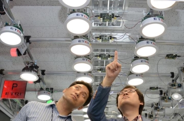
[Interview 1] "Is the next innovation in smartphones the camera? Then pay attention to LED communication technology"
LED communication technology is advancing rapidly alongside smart lighting. In 2011, under the leadership of Samsung Electronics and ETRI, standardization of visible light communication was achieved. In particular, LED-ID is a technology that enables transmission and reception of unique information through LED display-based screens and smart cameras. We met with Professor Young-min Jang from Kookmin University (photo), who is proceeding with standardization, to hear in detail about the progress of LED communication technology.
2016.01.18by
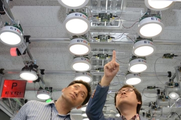
[Interview 2] "Is the camera the next innovation in smartphones? If so, pay attention to LED communication technology."
Advancement in LED communication technology is progressing rapidly alongside smart lighting. In 2011, standardization of visible light communication was achieved under the leadership of Samsung Electronics and ETRI. In particular, LED-ID is a technology that enables transmission and reception of unique information through LED display-based screens and smart cameras. We met with Professor Jang Young-min from Kookmin University (photo), who is leading the standardization efforts, to hear in detail about the progress of LED communication technology.
2016.01.29by
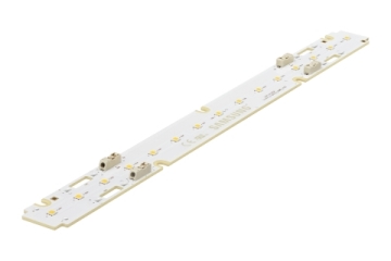
Samsung Electronics Launches LED Modules for Industrial Lighting
Samsung Electronics has launched 'inFlux,' a high luminous flux LED module optimized for industrial lighting, and is beginning its full-scale initiative to capture the LED module market. Luminous flux refers to the total amount of light emitted from a light source.
2016.02.02by
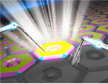
White LED, implemented with a single chip without using phosphors
A KAIST research team has developed a white LED manufacturing technology. Since this technology is a white LED manufacturing method that does not use phosphors, it is expected to contribute to advances in next-generation lighting and display technologies.
2016.02.25by
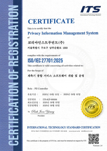
Korea Instrument, KOLAS Accredited Calibration Agency First to Simultaneously Acquire ISO/IEC 27,001·27,701
Korea Instrument has become the first among KOLAS accredited calibration agencies to simultaneously acquire ISO/IEC 27,001 and ISO/IEC 27,701 certifications. Through its proprietary platforms CWIZ Enterprise and CWIZ Partners, the company has embedded information security and personal data protection requirements across all business processes including customer information, equipment data, and calibration reports, with plans to continuously advance its management system through regular audits and security inspections.
2026.10.12by 배종인 기자











