


Toshiba Develops Electrostatic Discharge (ESD) Protection Device
 Published2016.06.20 06:51
Toshiba Corporation has developed an electrostatic discharge (ESD) protection device for analog power semiconductor applications.
This device is manufactured using advanced 0.13μm process technology, optimizing the transistor structure and significantly improving ESD characteristics. ESD protection capabilities have increased by up to four times, making it much more robust, and the standard deviation is only one-twelfth of that of existing devices.
Toshiba identified a transistor structure optimization mechanism that enables ESD strength through 3D simulation analysis. Toshiba announced these findings at the “ISPSD2016” international semiconductor symposium held in the Czech Republic on June 14, 2016.
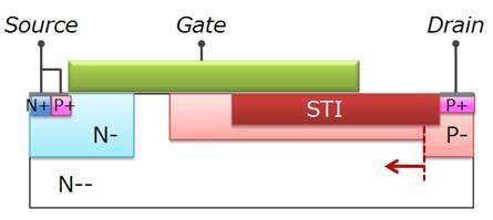
Since ESD current flow raises the local temperature inside silicon, semiconductor devices can be destroyed if an ESD surge is introduced from the human body or equipment. ESD protection devices must protect internal circuits, which is especially true for analog power semiconductor devices that require high rated voltages ranging from 10V to 100V.
In this case, the ESD protection device must secure a high current flow, which results in an increase in chip size. The reduction in size of ESD protection devices is linked to the problem of implementing more compact chips.
Toshiba used 3D simulation analysis of ESD to reveal that ESD-induced destruction occurs due to a rise in lattice temperature caused by current flow at the peak of the electric field.
By modifying the transistor structure to extend the low-resistance drain region toward the source and suppress silicon lateral resistance, current flow is diverted from the bottom of the drain toward the source and isolated at the peak of the electric field. It was found that this optimized design increases ESD strength by up to four times and reduces the standard deviation to one-twelfth. Additionally, the device size requiring HBM ±2000V was reduced by 68%.
Toshiba offers an advanced analog process platform utilizing 0.13μm process technology, which can be embedded in passive devices such as resistors and capacitors, as well as CMOS, DMOS, and bipolar transistors. Users can select the process suitable for each application from the following three process platforms: the “BiCD-0.13” (DMOS lineup up to 100V), primarily used in automotive applications; the “CD-0.13BL” (DMOS lineup up to 60V), primarily used in motor drivers; and the “CD-0.13” (DMOS lineup up to 40V), primarily used in power management ICs.
Toshiba plans to launch products using the CD-0.13 process with this technology applied in 2017 and continue to implement other process platforms to improve electrostatic discharge characteristics.

Comments
Related news
Toshiba Launches 4-Channel Power Amplifier IC to Prevent Speaker Fires
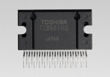
Toshiba Corporation's Storage & Electronic Devices Solutions Company announced on the 28th the launch of "TCB501HQ," a 4-channel power amplifier IC. This new IC features a built-in full-time offset detection circuit that detects speaker output offset voltage, which is a cause of speaker fires. It detects output DC offset voltage generated by leakage from input capacitors and other sources during sound playback, preventing speaker fires. The new IC employs a current feedback system of the type adopted in high-end hi-fi audio. This prevents audio quality degradation across a wide bandwidth and ensures stable sound quality.
2016.04.28by
Toshiba Announces PCI Express for Custom LSI Platforms
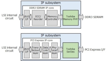
Toshiba Corporation's Storage and Device Solution Company announced the launch of PCI Express and DDR3 SDRAM IP subsystems. These products were jointly developed with Northwest Logic, a leading company providing high-performance, easy-to-use, and silicon-proven PCI Express and Memory Interface IP cores. These subsystems can be used on custom LSI platforms including ASICs and FFSA*4. The PCI Express core includes standards-compliant and fully-featured PCI Express 3.0/2.1/1.1 cores, high-performance scatter-gather DMA cores, and drivers (Linux & Windows). The DDR3 SDRAM Controller Core delivers high-bandwidth support through additional core full options such as ARM AMBA AXI, multi-port, reordering, ECC, and memory test support.
2016.06.03by 명세환 기자
SCCG for restoring receiver sensitivity of Toshiba wireless connection ICs
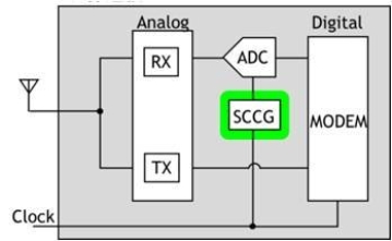
Toshiba Corporation has developed a spur canceled clock generator (SCCG) that restores receiver sensitivity in wireless connectivity ICs. The SCCG recovers receiver sensitivity by suppressing spurs, which are interference generated from clock signals, and achieves a receiver sensitivity of -93 dBm across all channels for Bluetooth® Smart ICs. Toshiba plans to present this technology at VLSI Circuits Symposium 2016, an international semiconductor device conference to be held in Honolulu, Hawaii on June 15.
2016.06.16by 명세환 기자

Intel Unveils Next-Generation 'Core Ultra Series 3' and vPro Platform for Enterprise PCs
Intel has officially unveiled the "Intel Core Ultra Series 3" for next-generation enterprise PCs and the latest vPro platform, addressing a wide range of demands from enterprise notebooks to high-performance workstations.
2026.03.26by 배종인 기자

ROHM Launches ESD Protection Diode Compatible with High-Speed Interfaces of 10Gbps or Higher
Semiconductor specialist ROHM has developed the 'RESDxVx series' of ESD (electrostatic discharge) protection diodes capable of responding to next-generation high-speed data communication environments exceeding 10Gbps, simultaneously enhancing both signal quality maintenance required in high-speed interfaces and IC protection performance.
2026.03.26by 배종인 기자











