


ams Announces New Version of Industrial Benchmark Process Design Kit
 Published2016.07.20 17:23
Provides a new “hitkit” design environment, high-density libraries, and enhanced transistor sets
ams (Korea Branch Representative Lee Jong-deok) announced a new version of its industrial benchmark process design kit (PDK).
The newly announced PDK is based on ams’s 180nm CMOS specialty process technology and is currently being manufactured at ams’s 200mm fab facility in Austria. The new PDK not only significantly enhances analog capabilities and device performance but also provides product developers with highly precise simulation models as a plug-and-play tool. Utilizing the first-ever fit design, this product supports the achievement of industry-required mission capabilities by continuously shortening development schedules.

ams’ “hitkit” design environment provides fully characterized passives, including 1.8V and 5.0V NMOS and PMOS devices (substrate-based, floating, low leakage, high threshold voltage options) and various capacitors. It includes an area-optimized high-density and low-power digital library with a gate density of up to 152 kGates/mm², an updated digital and analog I/O library with six metal layers, and an ESD protection cell with a maximum 8 kV HBM level.
It provides online memory generation services for OTP (One-Time Programmable) memory, RAM, and ROM, as well as complete configuration of Zero-Mask-Level-Adder EEPROM IP blocks (up to 8kbit).
A new hitkit based on Cadence®’s Virtuoso® Custom IC 6.1.6 supports design teams in significantly reducing time-to-market for highly competitive products in analog-intensive mixed-signal fields. Featuring high-precision simulation models as well as extraction and verification action sets for Calibre, Assura, and flexible SKILL-based PCells, this new hitkit provides a comprehensive design environment and a verified route for semiconductors. The 0.18 nm CMOS special process (“aC18”) is manufactured at ams’s state-of-the-art 200 mm fab facility in Austria, ensuring a very low defect rate and excellent yield.
"The implementation of aC18 technology in the manufacturing process at ams's Austrian fab has been a significant milestone," said Markus Wuchse, General Manager of ams's Full Service Foundry business unit. "Just as we have achieved with the 350nm process family in the past, with the announcement of the new hitkit, ams is now able to support foundry customers with rapid prototyping and high-quality production quantities of complex analog semiconductors in the 180nm process."
ams’s aC18 specialty process is ideally suited for sensors and sensor interface devices in various applications such as wearables, healthcare, home automation, smart cars, and Industry 4.0. This process enables the development of innovative solutions suitable for consumer electronics and industrial equipment for the Internet of Things (IoT) and smart cities. Prototype operation can begin immediately. Mass production is scheduled for July 2016.
Comments
Related news
ams Announces Interoperable Process Design Kit
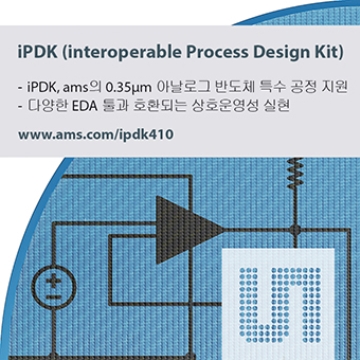
ams (Korea Representative Lee Jong-deok) announced that it has launched iPDK (interoperable process design kit), a mutually interoperable process design kit for its 0.35μm analog semiconductor specialty process, for the first time. The iPDK is based on an OpenAccess database and implements interoperability with various EDA vendor tools by using not only standard languages but also an integrated architecture.
2016.03.23by 신윤오 기자
ams Launches Precise Automotive Position Sensor
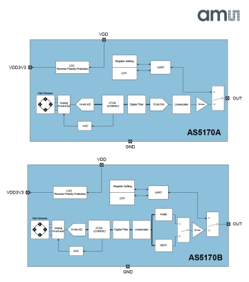
ams, a specialist in sensors and analog ICs, announced an expansion of its functional safety-compliant sensor portfolio. The newly launched sensor series is ams's first magnetic position sensor offered in System-in-Package (SiP) format. SiP is a space-saving package that can reduce system costs and enables sensor device utilization even in environments where PCB-based packages are prohibited. The new AS5170 and AS5171 sensors were developed for SEooC (Safety Element out of Context) product applications as defined by the ISO 26262 functional safety standard. The AS517x components, which provide comprehensive data path diagnostics as magnetic position sensors from ams, enable automotive system OEMs to achieve ISO 26262 system-level compliance.
2016.04.27by

ams Announces New Temperature Sensor Ideal for Wearable Devices
ams (Korea Branch Representative: Lee Jong-deok) announced the launch of the AS6200, a highly integrated digital temperature sensor that combines low power consumption and high precision functionality in a compact package at the industry's best levels. The AS6200, with dimensions of 1.6mm x 1mm, has a typical current consumption of 6μA at a measurement speed of 4 samples per second, and its digital measurement output has a precision of ±0.4°C. The AS6200, which is factory calibrated with precision, integrates the functions required in temperature sensing systems into a single chip, enabling users to easily design sensors even in space-constrained or battery-powered products.
2016.06.22by 명세환 기자

Intel Unveils Next-Generation 'Core Ultra Series 3' and vPro Platform for Enterprise PCs
Intel has officially unveiled the "Intel Core Ultra Series 3" for next-generation enterprise PCs and the latest vPro platform, addressing a wide range of demands from enterprise notebooks to high-performance workstations.
2026.03.26by 배종인 기자

ROHM Launches ESD Protection Diode Compatible with High-Speed Interfaces of 10Gbps or Higher
Semiconductor specialist ROHM has developed the 'RESDxVx series' of ESD (electrostatic discharge) protection diodes capable of responding to next-generation high-speed data communication environments exceeding 10Gbps, simultaneously enhancing both signal quality maintenance required in high-speed interfaces and IC protection performance.
2026.03.26by 배종인 기자











