


Toshiba Ships Samples of 64-Layer 3D Flash with Increased Capacity via Added Stacking
 Published2016.07.28 06:03
Toshiba Corporation has unveiled a next-generation BiCS FLASH™ 3D flash memory with a stacked cell structure*.
Sample shipments of the world's first 64-layer stacked product have begun. This new device incorporates 3-bit/cell (TLC) technology and has a capacity of 256 gigabits (32 gigabytes), serving as a demonstration of the potential of Toshiba's proprietary architecture. Toshiba plans to continue improving BiCS FLASH™ and aims to launch a 512-gigabit (64 gigabyte) 64-layer stacked product as its next goal.
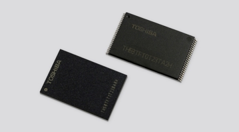
This product succeeds the existing 48-layer BiCS FLASH™ and utilizes a state-of-the-art 64-layer stacking process to achieve a 40% increase in capacity per chip area compared to the 48-layer process, while reducing the cost per bit and increasing the memory capacity produced per silicon wafer. The 64-layer BiCS FLASH™ can meet demanding performance specifications and can be used in various applications such as enterprise and consumer SSDs, smartphones, tablets, and memory cards.
Since unveiling the world's first prototype 3D flash memory technology in June 2007, Toshiba has continued to develop the technology. The company is currently dedicated to developing BiCS FLASH™ to meet the demands for increased capacity and reduced size.
Toshiba will produce the new 64-layer BiCS FLASH™ at New Fab 2 of its Yokkaichi Operations plant, which officially opened earlier this month. Mass production of the 64-layer BiCS FLASH™ is scheduled to begin in the first half of 2017.
Comments
Related news
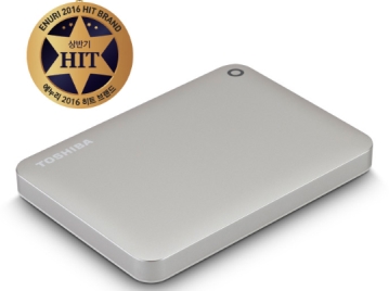
Toshiba Wins Hit Product Award in External Hard Drive Category Based on Unique Stability
Toshiba Electronics Korea (hereafter Toshiba) announced that it has been selected as the '2016 Hit Brand' in the external hard drive category by Enuri.com, a price comparison website. The Enuri Hit Brand selection was based on sales performance during the first half of this year, with 60 brand categories chosen across four sectors: computers, home appliances, digital devices, and lifestyle. The selection was determined through fair evaluation by specialized category managers (CM) based on Enuri.com's internal data, considering consumer satisfaction, interest level, and sales volume.
2016.07.08by 신윤오 기자
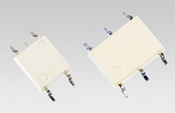
Toshiba Launches Compact Package Photorelay for High Current Control
Toshiba Corporation's Storage and Electronic Products Company has announced the launch of high-current control photocouplers with a current range of 1.7A to 4A in compact 2.54SOP4/2.54SOP6 packages. Shipments of the new product series (TLP3106, TLP3107, TLP3109, TLP3127) are beginning immediately, with application examples for the new lineup including programmable logic controllers (PLCs), battery management systems (BMS), and factory automation inverters.
2016.07.12by 신윤오 기자
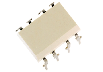
Toshiba Launches DIP8 Package Photorelay Driven by 5A High Current
Toshiba Corporation's Semiconductor & Storage Products Company has announced the addition of three new products to its photorelays lineup, which enables replacement of mechanical relays in industrial applications, including industry-leading 5A high-current-driven DIP8 package photorelays.
2016.07.22by 김수지 기자

Intel Unveils Next-Generation 'Core Ultra Series 3' and vPro Platform for Enterprise PCs
Intel has officially unveiled the "Intel Core Ultra Series 3" for next-generation enterprise PCs and the latest vPro platform, addressing a wide range of demands from enterprise notebooks to high-performance workstations.
2026.03.26by 배종인 기자

ROHM Launches ESD Protection Diode Compatible with High-Speed Interfaces of 10Gbps or Higher
Semiconductor specialist ROHM has developed the 'RESDxVx series' of ESD (electrostatic discharge) protection diodes capable of responding to next-generation high-speed data communication environments exceeding 10Gbps, simultaneously enhancing both signal quality maintenance required in high-speed interfaces and IC protection performance.
2026.03.26by 배종인 기자











