



High-Linearity I/Q Demodulator Announced with Enhanced Linearity and Receiver Performance
 Published2016.07.28 11:14
Linear Technology Korea (CEO Hong Sa-gwak) has announced the launch of a new high-linearity I/Q demodulator product (model: LTC5586) featuring over 1GHz bandwidth with –1dB flatness.
This product supports next-generation 5G wireless infrastructure equipment such as base stations, microwave backhaul, and digital predistortion correction (DPD) for software-defined radios (SDR), as well as other broadband receiver applications.
The LTC5586 provides a broadband RF input port. Using a single matching network, the product is matched to 50Ω in the 500MHz to 6GHz range and covers all LTE bands as well as newly emerging 3.6GHz and 5GHz 4.5G and 5G bands. To support operation in the 300MHz to 500MHz range, additional capacitors are required.
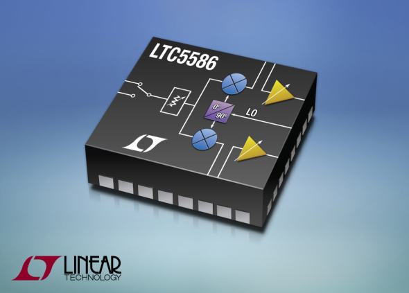
The device features built-in SPI-adjustable tuning capability, allowing the demodulator to set the LO input across the frequency range of 300MHz to 6GHz without external matching components. The new demodulator supports very high OIP2 of 80dBm and 60dBc sideband suppression, ensuring excellent receiver performance.
The LTC5586 is a true zero-IF design that directly demodulates broadband RF signals to baseband DC or low-IF coupling. The demodulator leverages the quadrature relationship between the two I and Q channels, and when both channels are sampled across a bandwidth equivalent to half the entire incoming RF bandwidth, all available information is fully captured. As a result, sampling rate and cost of the A/D converter (ADC) can be reduced.
At the front end, the LTC5586 features an RF switch selecting one of two inputs with an attenuator programmable through an on-chip serial bus. This front-end attenuator provides a gain control range of 31dB in 1dB steps, allowing the receiver to accommodate a wide range of signal inputs. The demodulator consists of I and Q mixers, each driven by its respective LO with a precise wideband quadrature phase shifter.
After signal demodulation, two programmable gain amplifiers provide gain to the I and Q baseband signal paths. Maximum gain of 7.7dB can be set through the serial port in 1dB steps, and the device can directly drive a pair of external A/D converters while the user optimally sets signal levels.
Additionally, the LTC5586 features proprietary on-chip tuning capability for simple calibration through the SPI serial port. Through this interface, users can adjust I and Q amplitude and phase balance, resulting in significantly simplified calibration that achieves excellent 60dB or better image rejection performance. The same interface can optimize IIP2, IIP3, HD2 (2nd harmonic distortion), and HD3 performance, improving overall linearity performance of the receiver. Since the device's baseband is DC-coupled, the DC offset voltage of this product can be zeroed across the entire baseband signal chain. The integrated total offset that is possible for as long as practical exists within the tuning range of the LTC5586.
The LTC5586 is supplied in a 5mm x 5mm plastic QFN package. The I and Q outputs feature 100Ω differential impedance and can directly drive a pair of interstage filters and external ADCs when terminated externally. This enables a compact solution with minimal external components required. The operating temperature range is specified from –40°C to 105°C. The LTC5586 is supplied at $7.79 per unit based on quantities of 1,000 pieces and is currently available in production volumes.
Related news
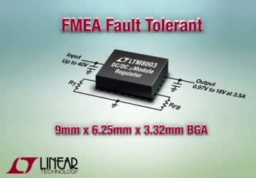
Linear Launches FMEA-Compliant 40V, 3.5A μModule Regulator
Linear Technology Korea (CEO Hong Sa-gwak) announced the launch of the LTM8003, a step-down DC/DC μModule® regulator featuring a 40V rated input voltage (42V absolute maximum) and 3.5A continuous (6A peak) output current. The LTM8003 pinout complies with FMEA (failure mode effects analysis), and therefore the output voltage is maintained at or below the regulation voltage even when a single pin is open, adjacent pins are shorted, or the output voltage is shorted to GND. The maximum junction temperature for the H-grade is 150°C, making it ideal for high-temperature or high-power automotive and industrial applications.
2016.07.01by 명세환 기자
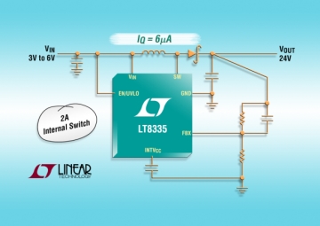
Linear, Step-Up DC/DC Converter with Integrated 2A 28V Switch Launched
Linear Technology Korea (CEO Hong Sa-kwak) announced the launch of LT8335, a current-mode, 2MHz step-up DC/DC converter with an integrated 2A, 28V switch. The product operates in an input voltage range of 3V to 25V and is suitable for applications that provide input sources from single-cell lithium-ion inputs to automotive input ranges. The LT8335 can be configured as a boost, SEPIC, or inverting converter.
2016.07.08by 홍보라 기자
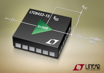
Linear Technology Announces Amplifier Delivering 47dBm OIP3 Linear Performance with Low Noise
Linear Technology Korea (CEO Hong Sa-kwak) has announced the launch of a wideband 15dB gain block amplifier (product name: LTC6433-15) that delivers outstanding linearity by providing 47dBm OIP3 (output third order intercept) and a noise figure of 3.22dB at 150MHz. This amplifier offers outstanding OP1dB (output 1dB compression point) of 19.2dBm. The LTC6433-15 is completely different from other gain block amplifier products typically designed using GaAs or pHEMT processes. FET technology has a high 1/f noise corner in the 20MHz to 30MHz band, which can result in elevated noise floor. This means it cannot be used at lower frequencies.
2016.07.22by 홍보라 기자

Intel Unveils Next-Generation 'Core Ultra Series 3' and vPro Platform for Enterprise PCs
Intel has officially unveiled the "Intel Core Ultra Series 3" for next-generation enterprise PCs and the latest vPro platform, addressing a wide range of demands from enterprise notebooks to high-performance workstations.
2026.03.26by 배종인 기자

ROHM Launches ESD Protection Diode Compatible with High-Speed Interfaces of 10Gbps or Higher
Semiconductor specialist ROHM has developed the 'RESDxVx series' of ESD (electrostatic discharge) protection diodes capable of responding to next-generation high-speed data communication environments exceeding 10Gbps, simultaneously enhancing both signal quality maintenance required in high-speed interfaces and IC protection performance.
2026.03.26by 배종인 기자











