


Samsung Electronics Develops Amorphous Graphene Technology Grown on Semiconductors
 Published2017.02.13 14:30
Developed jointly with Sungkyunkwan University, published in Science Advances
Professor Hwang Dong-mok and Dr. Lee Jae-hyun of the Department of Materials Science and Engineering at Sungkyunkwan University's College of Engineering, along with Executive Vice President Hwang Sung-woo and Dr. Joo Won-je of Samsung Electronics' Advanced Institute of Technology, announced that they have jointly developed the world's first source technology for "large-area single-atom-layer amorphous graphene synthesis" on semiconductor wafers.
In 2014, a joint research team from Sungkyunkwan University and Samsung Electronics developed a source technology for synthesizing single-crystal graphene on a semiconductor substrate over a large area. Through this follow-up research, they succeeded in synthesizing amorphous graphene, in which carbon atoms are randomly connected on a two-dimensional plane, over a large area by controlling the interatomic defect structure within the two-dimensional material.

▲ Amorphous graphene
Professor Hwang Dong-mok predicted, “This achievement is significant in that it greatly expands the scope of 2D materials, which are emerging as core materials for next-generation industries, and it will be possible to pioneer new application fields based on the new characteristics of amorphous 2D materials, which are different from existing crystalline 2D materials.”
The paper on these research results is published in Science AdvanceIt was published on the online edition of ces) on the 10th.
Comments
Related news
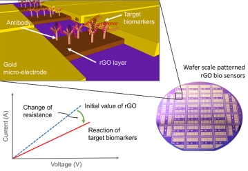
Diagnosing diseases with a single drop of blood: Development of high-sensitivity graphene biosensors takes a step closer
Recently, domestic researchers successfully implemented graphene, known as the 'dream material,' on a large-area panel (4-inch wafer) and developed a high-sensitivity biosensor fabrication technology capable of diagnosing various diseases and conditions. Dr. Hwang Gyo-seon's team at the Biomicrosystems Research Division of the Korea Institute of Science and Technology (KIST, President Lee Byung-kwon) fabricated a graphene biosensor with precisely implemented patterns of tens of micrometers (one hundred-thousandths to one millionth of a meter) by applying semiconductor processing technology.
2016.08.16by 신윤오 기자
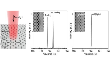
Implementing future optical computers using light-absorbing graphene properties
The Ministry of Science, ICT and Future Planning (Minister Choi Yang-hee) announced that "domestic researchers have developed technology that can freely change the color of nanolasers, which are small lasers in the nanometer size range, by utilizing graphene's light-absorbing properties." Graphene is a material with an atomic-scale honeycomb structure made of carbon atoms. It has excellent thermal conductivity, is transparent, and possesses excellent stretchability, making its application fields very diverse. However, it is known to be difficult to use in optical devices that utilize light due to its light-absorbing properties. Nanolasers are lasers that use light-confining devices in the tens to hundreds of nanometer size range.
2017.01.12by 신윤오 기자
[Interview] Will the path to mass production of the dream nanomaterial, graphene, open?
Is there no new method to mass-produce graphene, which is attracting attention as a next-generation advanced material, at low cost and high quality? The high-quality graphene mass production technology developed by the Graphene Materials Team (Principal Researcher Yang Woo-seok) at the Electronics and Telecommunications Research Institute (KETI) presents a solution to this demand. The technology developed by the Graphene Materials Team demonstrates the possibility of controlling interlayer insertion speed through a reactor utilizing shear stress, explosion reaction control, and continuous production. Graphene is a single layer composed of hexagonal carbon atoms and is an advanced material with superior properties—including high strength, electron mobility, and electrical conductivity—among all existing materials. However, mass production technology for single or few-layer graphene with uniformity has not yet been developed globally, presenting challenges for industrialization.
2017.01.16by 김지혜 기자

Intel Unveils Next-Generation 'Core Ultra Series 3' and vPro Platform for Enterprise PCs
Intel has officially unveiled the "Intel Core Ultra Series 3" for next-generation enterprise PCs and the latest vPro platform, addressing a wide range of demands from enterprise notebooks to high-performance workstations.
2026.03.26by 배종인 기자

ROHM Launches ESD Protection Diode Compatible with High-Speed Interfaces of 10Gbps or Higher
Semiconductor specialist ROHM has developed the 'RESDxVx series' of ESD (electrostatic discharge) protection diodes capable of responding to next-generation high-speed data communication environments exceeding 10Gbps, simultaneously enhancing both signal quality maintenance required in high-speed interfaces and IC protection performance.
2026.03.26by 배종인 기자











