


KLA-Tencor, Introduction to Integrated Circuit Equipment Technology Measurement Systems
 Published2017.03.21 11:28
KLA-Tencor Corporation announced the Archer 600 overlay metrology system, the WaferSight PWG2 pattern wafer geometry measurement system, the SpectraShape 10K optical critical dimension measurement system, and the SensArray HighTemp 4mm field temperature measurement system as measurement systems that enable the development and mass manufacturing of sub-10nm integrated circuits. The four new systems enable support for advanced patterning technologies such as self-aligned quadruple patterning (SAQP) and extreme ultraviolet (EUV) lithography.
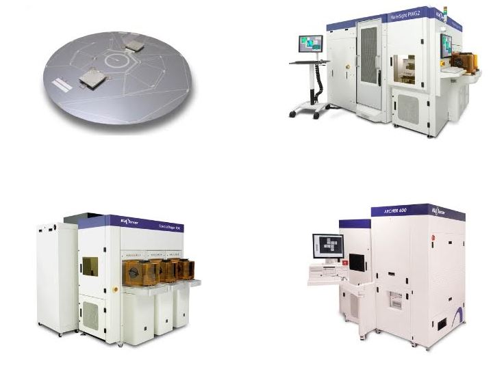
Archer 600 extends image-based overlay metrology technology to new optical and measurement targets, enabling chip manufacturers to achieve on-product overlay (OPO) errors of less than 3 nm for advanced logic and memory devices.
WaferSight PWG2 generates comprehensive wafer stress and geometry data, enabling film deposition, thermal strengthening, monitoring, and matching. By increasing wafer sampling during production through improved productivity, it helps chip manufacturers identify and correct process-induced wafer stress variations that may affect patterning processes and yield. In addition, wafer shape data can be used to reduce overlay errors caused by wafer deformation due to the high stacking structure of 3D NAND in the exposure equipment.
The SpectraShape 10K optical-based metrology system measures the critical dimension (CD) and three-dimensional structure of complex IC device structures associated with etching, chemical mechanical planarization (CMP), and other process steps. It employs optical technology that includes a new polarization function, an ellipsometer equipped with multiple angles of incidence, and a new high-intensity light source TruNI optical coherence thickness meter.
SensArray HighTemp 4mm wireless wafers provide temporal and spatial temperature information for advanced T/F processes. With a temperature range of 20°C to 400°C, process characteristics and equipment verification are possible using thermal variations that can affect process and pattern performance.
"To understand patterning errors, chip manufacturers must quantify process variables, identify sources, and address root problems," said Oreste Donzella, Marketing Director at KLA-Tencor. "The new metrology system plays a key role in driving 193i multi-patterning performance and providing the foundation for early EUV lithography results."
관련뉴스
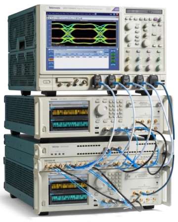
Tektronix Unveils Integrated Receiver Test Solution for High-End Applications
텍트로닉스는 D-PHY v.2.0 규격과 C-PHY v1.1 리시버 테스트 규격을 지원하는 리시버 테스트 솔루션을 발표했다. 이로 인해 텍트로닉스는 신호 품질과 디버깅 및 마진 테스트를 위한 포괄적인 측정 기능을 통해 자율 주행 시스템 또는 차량 내 인포테인먼트 등의 분야에서 MIPI 설계업체들의 PHY 리시버 테스트 설정을 간소화하고 테스트 실행 속도를 더 높일 수 있게 되었다고 전했다.
2017.02.08by 김지혜 기자

[MAXIM Point!] Extend Battery Life: Consider Standby Current First
Smart and connected products continue to shrink in size while expectations for functionality and performance keep rising. Batteries are also following this trend, becoming smaller while offering longer operational life. Low standby current is critical for effectively extending battery life. Recently, medical patches have emerged for body temperature measurement, insulin delivery, and heart rate monitoring. For these devices, reliable long-term operation is paramount. However, these devices are often stored for extended periods in supply rooms and pharmaceutical warehouses before being used. Additionally, smartwatches, earbuds, and video game controllers must operate for extended durations after rapid charging.
2017.03.17by 김지혜 기자
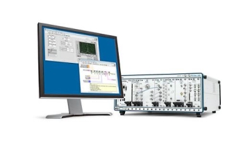
NI Releases Software to Speed PXI RF Tests by Up to 33%
National Instruments announced NI-RFmx 2.2, the latest version of advanced measurement software for PXI RF test systems. When used together with the second-generation PXI vector signal transceiver, this software enables testing of 4.5G/5G RF components such as transceivers and amplifiers by leveraging carrier aggregation architectures that utilize two frequencies or different networks.
2017.03.20by 김자영 기자

Intel Unveils Next-Generation 'Core Ultra Series 3' and vPro Platform for Enterprise PCs
Intel has officially unveiled the "Intel Core Ultra Series 3" for next-generation enterprise PCs and the latest vPro platform, addressing a wide range of demands from enterprise notebooks to high-performance workstations.
2026.03.26by 배종인 기자

ROHM Launches ESD Protection Diode Compatible with High-Speed Interfaces of 10Gbps or Higher
반도체 전문 기업 로옴(ROHM)이 10Gbps를 넘어서는 차세대 고속 데이터 통신 환경에 대응할 수 있는 ESD(정전기 방전) 보호 다이오드 ‘RESDxVx 시리즈’를 개발하며, 고속 인터페이스에서 요구되는 신호 품질 유지와 IC 보호 성능을 동시에 끌어올렸다.
2026.03.26by 배종인 기자











