



Lattice Announces Embedded Vision Development Kit to Optimize Mobile System Design
 Published2017.05.02 10:45
Accelerating the development of intelligent vision devices for edge equipment
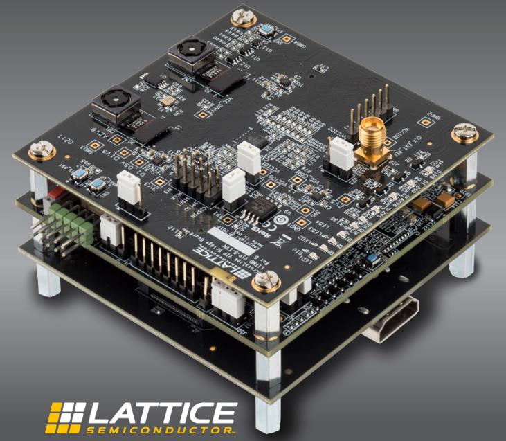
Lattice Semiconductor announced the launch of the Embedded Vision Development Kit, the first development kit optimized for mobile-influenced system designs requiring a flexible, low-cost, low-power image processing architecture.
This solution, which integrates a combination of Lattice’s FPGA, ASSP, and programmable ASSP (pASSP) products into a single modular platform, provides the flexibility and energy efficiency required by various embedded vision applications in the industrial, automotive, and consumer markets.
By combining the CrossLink pASSP mobile bridging device, the ECP5 low-power small form factor FPGA, and the high-bandwidth, high-resolution HDMI ASSP, Lattice provides a solution that accelerates the development of intelligent vision devices used in edge equipment.
Deepak Boppana, Director at Lattice Semiconductor, stated, “As intelligent edge computing increases, the number of applications requiring integrated embedded vision technology will continue to grow,” adding, “Lattice’s embedded vision development kits will accelerate the adoption of mobile-related applications in fields such as machine vision, smart control cameras, robotics, AR/VR, drones, and advanced driver assistance systems (ADAS).”r />
The CrossLink input board includes a dual-camera HD image sensor supporting the MIPI CSI-2 interface, eliminating the need for additional external video sources. The ECP5-based board enables low-power pre- and post-processing and supports Helion Vision's HD Image Signal Processor (ISP) IP. It also includes a NanoVesta connector that supports external image sensor video input. The HDMI output board, based on the Sil1136—a version that does not support HDCP—supports connectivity for standard HDMI displays.
Comments
Related news
Lattice Launches World's Smallest FPGA with Integrated Memory and DSP
Lattice Semiconductor (Branch Manager Lee Jong-hwa) announced the launch of the new iCE40 UltraPlus™ FPGA series. The iCE40 UltraPlus product is one of the most energy-efficient programmable mobile heterogeneous computing (MHC) solutions in the industry.
2016.12.13by 신윤오 기자

Lattice Semiconductor and TPCAST Deliver Immersive Wireless VR Experiences
Lattice Semiconductor and TPCAST announced that they have entered into a partnership to provide wireless solutions for head-mounted display (HMD) based virtual reality (VR) systems. Lattice's WirelessHD solution and FPGA and ASSP products are exclusively provided for TPCAST's VR applications that require low-latency, high-bandwidth wireless video transmission.
2017.01.24by 김지혜 기자
Lattice Semiconductor Expands Programmable ASSP Solution Supporting Video Bridging Function
Lattice Semiconductor announced that it has expanded its CrossLink™ programmable ASSP (pASSP) solution to support new video bridging capabilities. Lattice stated that the solution comprises three CrossLink IP (intellectual property) blocks and two CrossLink demo platforms, with each of the two demo platforms capable of demonstrating interface bridging from MIPI® DSI to LVDS and from CMOS to MIPI CSI-2 respectively. Regarding the solution expansion, the company optimized existing CrossLink IP to reduce logic resource utilization and lower power consumption.
2017.02.22by 김지혜 기자

Intel Unveils Next-Generation 'Core Ultra Series 3' and vPro Platform for Enterprise PCs
Intel has officially unveiled the "Intel Core Ultra Series 3" for next-generation enterprise PCs and the latest vPro platform, addressing a wide range of demands from enterprise notebooks to high-performance workstations.
2026.03.26by 배종인 기자

ROHM Launches ESD Protection Diode Compatible with High-Speed Interfaces of 10Gbps or Higher
Semiconductor specialist ROHM has developed the 'RESDxVx series' of ESD (electrostatic discharge) protection diodes capable of responding to next-generation high-speed data communication environments exceeding 10Gbps, simultaneously enhancing both signal quality maintenance required in high-speed interfaces and IC protection performance.
2026.03.26by 배종인 기자











