


Flexible OLEDs Must Improve Lifespan and Efficiency to Achieve Mass Adoption
 Published2017.05.08 15:28
Encapsulation technology is key to making thin, light, and flexible OLEDs.
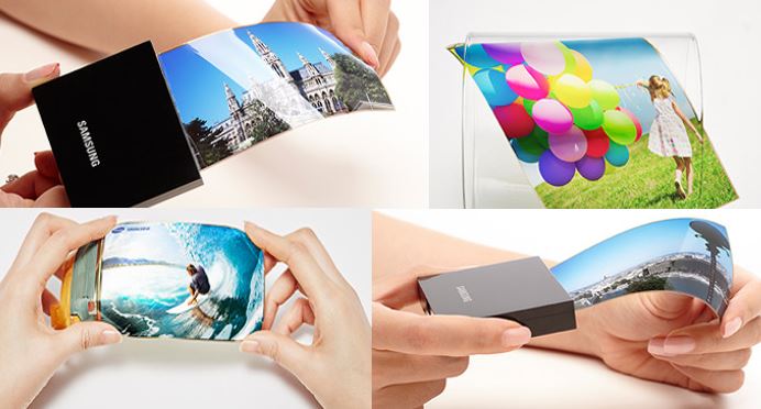
Displays are now entering the era of 'flexibility.' As interest shifts toward flexibility, Plastic Organic Light-Emitting Diodes (POLED) are gaining attention. According to market research firm IHS Market, OLEDs have caught up with Liquid Crystal Displays (LCDs), which dominate the smartphone display market, and with the demand for flexible OLED panels increasing rapidly, it is predicted that they will surpass flat-panel OLED panels in the third quarter of this year.
Compared to LEDs, OLEDs allow users to adjust color temperature, color, and brightness, and because they are surface light sources that emit light from all sides, they have a wide heat dissipation area, making them relatively free from heat issues. Assuming operation in a typical environment, heat sinks are not required, and transparency is possible due to the thin film thickness. Since they can be made of plastic instead of glass, they can also be bent.
The unresolved issues in OLED technology are efficiency, lifespan, light extraction, and price. Although OLEDs can theoretically achieve a luminous efficiency of up to 190 lm/W, they are currently at a level similar to LEDs, around 70 lm/W. The lifespan is possible up to 10,000 hours, but to compete with LEDs, it needs to be 30,000 hours.
In OLEDs, the electron transport layer, emissive layer, hole transport layer, and hole injection layer between the cathode (which acts as a reflective layer for injecting electrons) and the anode (which acts as a positive layer for injecting holes) are made of organic materials. Light is generated by the energy produced when holes (+) and electric charges (-) collide in the emissive layer. At this time, fluorescence and phosphorescence are emitted, and the light efficiency is determined by the ratio.
In the emissive layer, light-emitting particles receive energy generated by the combination of charges and holes and become excited. If the excited particles pass through a singlet state, it is fluorescence, and if they pass through a triplet state, it is phosphorescence. Theoretically, the internal quantum efficiency of fluorescence is 25%. This is the same regardless of which existing material is used.
Research on materials has been conducted as a method to utilize triplet particles to increase efficiency. Phosphorescence can be utilized by using heavy metals such as iridium (Ir), platinum (Pt), and titanium (Ti). The theoretical internal quantum efficiency of phosphorescence is 100%. Currently, materials capable of utilizing both fluorescence and phosphorescence are being used. However, since heavy metals are expensive to use as materials, TADF (Thermally activated delayed fluorescence) is being researched as an alternative.
TADF is a method of transferring the energy of a triplet to a singlet with relatively higher energy, which can be achieved by making the thermal energy difference between the singlet and triplet small. Although this method is not yet used by companies, it is being researched to replace heavy metals with an internal quantum efficiency of 100%.
The important thing in bagging technology is blocking moisture and oxygen.
Because the layers between the anode and cathode of OLEDs are made of organic materials, they are susceptible to contamination from oxygen, moisture, and particles. Encapsulation is a technology that prevents contaminant particles from entering the layers, and it is an important technology for lowering production costs and extending lifespan.
If encapsulation technology is not properly applied, black spots will form due to external factors, causing the area where light does not emanate to gradually expand. External factors are broadly classified into four categories, among which blocking moisture and oxygen is the most important. Oxygen and moisture enter through holes of approximately 2 to 3 nanometers that form during the thin-film process. However, even without holes, oxygen and moisture can dissolve into the barrier film due to migration driven by concentration differences. This can be resolved by extending the time it takes for electrons to reach the electron transport layer from the outside to the desired lifespan.
Generally, since water molecules are smaller than oxygen molecules, blocking moisture also blocks oxygen. The lower the amount of moisture passing through the film, the lower the water vapor transmission rate (WVTR), and the more organic matter is present, the more stringent the requirements become. The required moisture permeability for flexible OLEDs is about 10⁻⁶ .
The CAN method currently on the market involves making a lid out of metal or glass, covering it with an organic layer, and sealing the gaps on the sides with epoxy. While it has the advantages of low technical difficulty and low equipment investment costs, it has the disadvantages of taking a long time because the materials and lid must be manufactured separately, and the glass is thick so it cannot be bent.
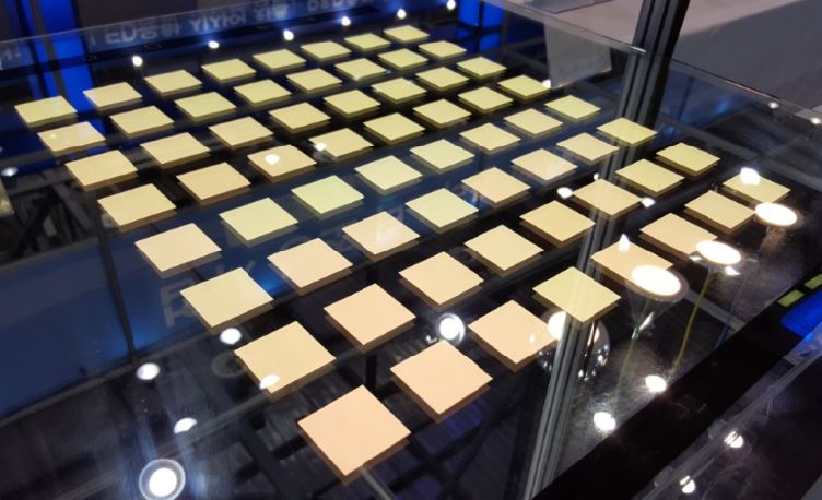
The TFE method involves stacking organic and inorganic materials alternately, which results in a thicker structure. Nevertheless, organic materials are used because they are susceptible to oxygen and moisture; stacking only inorganic materials would cause stress and lead to cracking. The organic material acts to alleviate this stress and smooth out uneven surfaces. Additionally, the organic material provides flexibility in the middle when the structure is bent.
Sputter and plasma CVD methods are preferred when producing TFE. Sputtering is used because it is inexpensive and allows for large-area processing. While CVD involves high process temperatures that substrates cannot withstand and affect organic materials, plasma CVD is used because of its relatively lower process temperatures. Although ALD (Atomic Layer Deposition) is not used for mass production, it has the advantages of producing dense films, covering uneven surfaces, and allowing for thin films. However, it involves high process temperatures and takes a long time.
Company S's recent product consists of five layers, with three organic layers and two inorganic layers. Research is underway to reduce this to three layers, with two organic layers and one inorganic layer.
Professor Joo Byung-kwon of the School of Electrical, Electronic and Radio Engineering at Korea University stated, “Encapsulation technology is crucial for creating thin, lightweight, and flexible OLEDs,” adding, “Barrier films are essential for plastic encapsulation technology. To achieve large-area displays at low costs, it is necessary to develop a solution-processed encapsulation method.”
Comments
Related news
Can Graphene Overcome the Limitations of Flexible Displays?
While there are ongoing discussions about foldable and flexible displays, what is the reason for the slow development of flexible displays? At a seminar on flexible display technology trends and issues held at KINTEX in Ilsan on the 17th, Dr. Kim Myeong-jong of the Korea Institute of Science and Technology (KIST), who gave a keynote presentation, stated, "Going forward, displays will be based on OLED and will move toward larger sizes, transparency, and flatness," and added, "Large-area CVD graphene is being applied in various fields, and since it is also used as a transparent electrode, it can be utilized in flexible and transparent displays as well."
2017.02.27by 김지혜 기자
ETRI to Use Graphene Instead of ITO in Displays
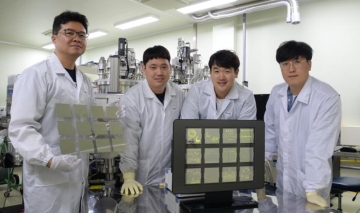
ETRI (Electronics and Telecommunications Research Institute) has successfully developed a display by creating electrodes using graphene, referred to as a dream material, instead of indium tin oxide (ITO), which has been widely used as electrodes for conventional OLED displays. The display substrate developed by the research team measures 370mm x 470mm, which is approximately the size of a 19-inch monitor. The graphene electrode thickness is 5 nanometers (nm) or less. ETRI anticipates that combining graphene with a flexible substrate will enable the implementation of thin and flexible displays. If realized, this could serve as a core technology applicable to the manufacturing of wearable devices that can be applied to clothing and skin.
2017.04.17by 김지혜 기자

Intel Unveils Next-Generation 'Core Ultra Series 3' and vPro Platform for Enterprise PCs
Intel has officially unveiled the "Intel Core Ultra Series 3" for next-generation enterprise PCs and the latest vPro platform, addressing a wide range of demands from enterprise notebooks to high-performance workstations.
2026.03.26by 배종인 기자

ROHM Launches ESD Protection Diode Compatible with High-Speed Interfaces of 10Gbps or Higher
Semiconductor specialist ROHM has developed the 'RESDxVx series' of ESD (electrostatic discharge) protection diodes capable of responding to next-generation high-speed data communication environments exceeding 10Gbps, simultaneously enhancing both signal quality maintenance required in high-speed interfaces and IC protection performance.
2026.03.26by 배종인 기자

ST Launches 75V Drive IC Targeting 48V Industrial Motor Driving
ST Microelectronics has unveiled the 'STSPIN9P' series of 75V motor drive ICs tailored for 48V-class industrial drive system design. The new product family is characterized by half-bridge and full-bridge configurations that enable design scalability according to motor type and output conditions. Power supply circuits, protection functions, and current sensing circuits are integrated on-chip to simplify system configuration, and the devices are designed to support applications up to 500W maximum. The company plans to provide reference designs and demo boards to support development and evaluation in industrial automation, robotics, pumps, fans, lighting, and textile machinery.
2026.03.26by 배종인 기자











