



Samsung Electronics Expands 4th Generation V-NAND Lineup by Overcoming Limitations of 3D Stacking Technology
 Published2017.06.15 15:59
Secured 1 Tera-bit V-NAND Core Technology
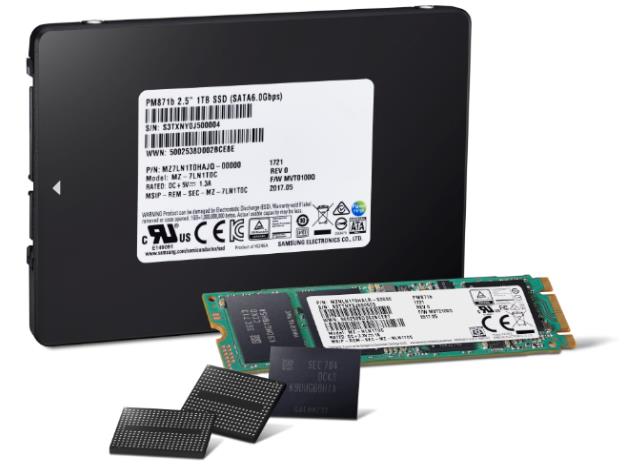
Samsung Electronics is expanding its 4th generation V-NAND lineup to the entire range of NAND products, including servers, PCs, and mobile devices, by beginning full-scale mass production of the '4th generation (64-layer) 256-gigabit (Gb) 3-bit V-NAND flash,' which delivers the world's highest performance and high reliability.
Samsung Electronics plans to expand the use of 4th generation V-NAND for mobile eUFS, consumer SSDs, and memory cards, following the 4th generation 256Gb V-NAND-based SSDs that began supplying to global B2B customers last January, and increase the monthly production share to over 50% within this year to meet the growing demand from global customers.
Three innovative technologies, including 'ultra-high integration cell structure and process', 'ultra-high speed operation circuit design', and 'ultra-high reliability CTF thin film formation', have been applied to the 4th generation (64-layer) V-NAND, improving speed, productivity, and power efficiency by more than 30% compared to the 3rd generation (48-layer) product.
V-NAND features a '3D (cylindrical) CTF cell structure' in which tens of layers are stacked to create data storage cells, and billions of tiny holes are uniformly drilled from top to bottom to vertically stack the cells.
However, stacking technology had physical limitations, such as the formed structure becoming distorted or differences in characteristics between the top and bottom cells appearing as the number of layers increased. In response, Samsung Electronics developed a "9-Hole" ultra-high-density cell structure and process technology to overcome limitations by forming a uniform hole pattern on each layer and distributing the load across the entire structure.
With this, Samsung Electronics has also secured the core technology to usher in the era of '1 Tera-bit V-NAND,' which stores more than 1 trillion pieces of information on a single semiconductor chip, by overcoming the vertical stacking limit of over 90 layers with the 4th generation V-NAND.
The 4th generation (64-layer) V-NAND not only has faster speeds but also lowered the operating voltage from 3.3V to 2.5V, increasing total power consumption efficiency by more than 30%.
In particular, by forming a Charge Trap Flash (CTF) thin film that can be controlled at the atomic level, the cell size was reduced while the write and erase characteristics lifespan was increased, and a control technology (channel thinning) that minimizes data interference between cells was also implemented, improving reliability by 20% compared to the 3rd generation.
Kyung-Hyeon Kye, Executive Vice President of the Flash Development Office at Samsung Electronics' Memory Business Division, stated, "All employees have dedicated themselves to developing innovative technologies to accelerate the era of Tera V-NAND," adding, "Going forward, we will continue to develop next-generation products in a timely manner to provide solutions that enhance user satisfaction for global IT companies and consumers."
Comments
Related news

Samsung Electronics to Install Smart Signage in Movie Theaters Nationwide
Samsung Electronics has installed smart signage at 50 CGV cinemas nationwide. Customers visiting the CGV cinemas can view various information through Samsung's smart signage, including movie trailers, advertisements, theater information, ticketing, and entrance guidance. Samsung Electronics has installed approximately 500 units of video wall-type signage that can be combined with multiple displays to function as a large screen, as well as various products including large-format UHD signage at 50 CGV cinemas nationwide, including locations in Wangsimni, Gangnam, Suwon, Daejeon, and Centum City in Busan. The 46-inch and 55-inch video wall-type smart signage and the large 85-inch UHD signage installed this time feature durability that poses no problems even with continuous 24-hour operation throughout the week, and support high brightness of 500 nits to display various content clearly even in dark spaces.
2017.06.07by 김지혜 기자
Samsung Electronics Launches HDR Gaming Monitor
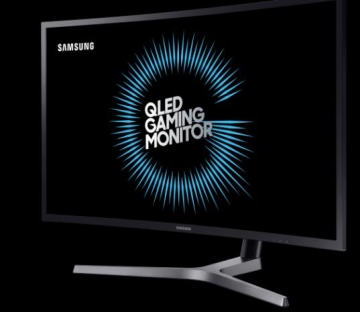
Samsung Electronics announced the launch of the CHG70 (27-inch and 31.5-inch) 2017 QLED gaming monitor with HDR (High Dynamic Range) functionality in the Korean market. The CHG70 is an upgraded product of the quantum dot curved gaming monitor (CFG70) that was launched last year, and it has been released with HDR technology applied. The CHG70 implements sRGB 125%, enabling high-level color gamut representation, and also supports up to 95% of DCI-P3 (Digital Cinema Color Standard), which is the production standard for major Hollywood studios, thereby clearly expressing fine details that conventional monitors could not represent.
2017.06.12by 김지혜 기자
Samsung Electronics Unveils Smart Signage Equipped with Tizen OS 3.0
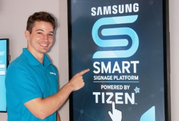
Samsung Electronics will debut its 2017 Samsung Smart Signage at Infocomm 2017, the world's largest display exhibition, held from June 14 to 16 in Orlando, United States, and will begin targeting the North American market. The 2017 Samsung Smart Signage features an enhanced graphics engine and hardware, and is equipped with Tizen 3.0, a Linux-based open-source operating system.
2017.06.14by 신윤오 기자

Intel Unveils Next-Generation 'Core Ultra Series 3' and vPro Platform for Enterprise PCs
Intel has officially unveiled the "Intel Core Ultra Series 3" for next-generation enterprise PCs and the latest vPro platform, addressing a wide range of demands from enterprise notebooks to high-performance workstations.
2026.03.26by 배종인 기자

ROHM Launches ESD Protection Diode Compatible with High-Speed Interfaces of 10Gbps or Higher
Semiconductor specialist ROHM has developed the 'RESDxVx series' of ESD (electrostatic discharge) protection diodes capable of responding to next-generation high-speed data communication environments exceeding 10Gbps, simultaneously enhancing both signal quality maintenance required in high-speed interfaces and IC protection performance.
2026.03.26by 배종인 기자











