



Western Digital Develops Next-Generation 96-Layer Vertically Stacked 3D NAND Technology
 Published2017.06.29 13:57
Sampling will begin in the second half of 2017, and trial production will begin in mid-2018.
Western Digital announced the successful development of its next-generation 96-layer vertically stacked 3D NAND technology, 'BiCS4'.
Jointly developed with Western Digital's technology and manufacturing partner, Toshiba, BiCS4 will initially be produced as a 256Gb (gigabit) chip, with future shipments in various capacities, including a single 1Tb (terabit) chip. It will be available in 3-bit-per-cell (TLC) and 4-bit-per-cell (QLC) architectures, with OEM customer sampling scheduled for the second half of 2017, with trial production expected in mid-2018.
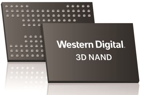
“The successful development of the industry’s first 96-layer 3D NAND technology further solidifies Western Digital’s leadership and technology roadmap in NAND flash,” said Siva Sivaram, senior vice president of memory technology at Western Digital. “With our 3D NAND portfolio that delivers the highest capacity, performance and reliability at a reasonable cost, we will address the needs of all NAND flash markets, spanning consumer, mobile, computing and data center.”
Meanwhile, Western Digital is accelerating its robust manufacturing operations, actively continuing production of NAND flash memory, including 3D NAND, at its joint venture manufacturing facility in Japan. This year, production of its 64-layer 3D NAND technology, "BiCS3," is expected to account for more than 75% of total 3D NAND supply. In particular, the joint venture manufacturing facility, including its partner Toshiba, is expected to record the highest production volume of 64-layer 3D NAND in the industry this year.
Comments
Related news
China's Shift from DRAM to NAND: Can Korea's 3D NAND Compete?
As the semiconductor market boom continues, Gartner, an IT market research firm, stated in a report on the 14th that "market growth is expected to continue through next year due to price increases and production volume growth in DRAM and NAND flash memory." IHS Markit senior research analyst Len Jelinek forecasted that "due to the large-capacity trend in IT devices, the amount of memory semiconductors installed in devices is increasing, and the memory semiconductor market growth rate will reach 30.3% this year." The system semiconductor market is expected to grow 10.5% year-over-year, and microcontroller units (MCU) are anticipated to show 6.7% growth driven by autonomous vehicle development. The overall memory market is projected to show growth through 2018, but from 2019 onwards, it is expected to slow due to variables such as China's government semiconductor industry policies. Mirae Asset Daewoo analyst Do Hyun-woo anticipated that the 2017 semiconductor equipment market will continue following last year's growth, with DRAM, foundry, and backend processes leading to overall 6% growth. The DRAM equipment market saw investment decrease at 23% last year, but this year investment is expected to increase by 15%, and due to memory market influence, investment will concentrate particularly in the second half. As Samsung Electronics and SK Hynix increase production volume of 18nm DRAM and invest in 17nm DRAM, equipment demand is predicted to increase. The NAND equipment market is expected to decline 4-5% compared to last year, as concentrated new capacity investments from Samsung Electronics, Toshiba, and Micron occurred in 2016. Samsung Electronics in particular invested heavily in 3D NAND flash at its Pyeongtaek plant last year, with plans to mass-produce 64-layer 3D NAND in the first half of this year. SK Hynix is preparing M14 3D NAND flash on the second floor of its Icheon plant this year, with plans to mass-produce 72-layer 3D NAND in the second half.
2017.05.01by 김지혜 기자
3D NAND on the Rise, Finding Processes and Materials to Solve Stacking Challenges
With 3D NAND supply volumes expected to surpass 2D NAND this year, interest is growing in the processes and materials required for stacking 3D NAND. On the 18th, the Semiconductor Electronic Materials Technology Conference (SMC, Strategic Materials Conference), hosted by the International Semiconductor Equipment and Materials Institute, was held under the theme "Scaling Challenges-The Future of Materials," discussing semiconductor material challenges for next-generation memory, market outlook for semiconductor materials, key process material technologies, and DRAM prospects. Sung-hyun Hong, Executive Director of Ram Research Korea, who presented, addressed the problems that arise as 3D NAND is stacked: "As the number of layers increases, the height becomes extremely high. If the structure is not harmonious, stress changes become severe. When stress becomes severe, the wafer bends, making handling difficult in subsequent processes."
2017.05.22by 김지혜 기자
Western Digital Announces 64-Layer 3D NAND-Based SSDs for Consumer Market
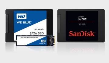
Western Digital announced the world's first launch of two client SSDs based on 64-layer 3D NAND technology: 'WD Blue 3D NAND SATA SSD' and 'SanDisk Ultra 3D SSD'.
2017.05.31by 신윤오 기자
.jpg)
SalePoint Signs Multi-Year Partnership Agreement with AWS… Promoting Identity Security that Integrates Even AI Agents
Sailpoint has entered into a multi-year strategic partnership agreement with AWS and is moving forward with establishing an integrated governance system that manages both human and non-human identities together. The plan is to consistently manage access permissions in an environment where AI agents are increasing as work execution entities, while applying the principle of least privilege and automated policy enforcement. The two companies plan to jointly expand capabilities to manage the identities of various entities, including AI agents, within a single layer in the AWS environment. This collaboration is interpreted as a move to design security and governance together in corporate environments where AI adoption is expanding.
2026.03.26by 배종인 기자
.png)
Databricks Unveils Open AI Security Monitoring 'Lakewatch'
Databricks entered the security market on March 24 by unveiling LakeWatch, an open-source agentic SIEM. The core functionality of this product is to integrate and analyze security, IT, and business data in a single environment to support AI-based threat detection and investigation. The company explained that it reduces the limitations of existing security operations centers, which have had to forgo some data due to high cost structures, and enables large-scale data analysis and automation based on open formats and ecosystems. LakeWatch is currently offered as a private preview, with Adobe and Dropbox mentioned as early customers. Databricks also announced an expanded partnership with Anthropic as well as the acquisition of Antimatter and SiftD.ai.
2026.03.26by 배종인 기자











