



Toshiba Develops 3D Flash Memory with TSV Technology Applied
 Published2017.07.13 15:12
Toshiba Memory Corporation has developed 3D flash memory with TSV technology applied for the first time in the world
Toshiba Memory Corporation announced the development of BiCS FLASH 3D flash memory by applying TSV (Through Silicon Via) technology adopted with triple-level cell (TLC) technology that stores 3 bits per cell.
Product samples are scheduled to be disclosed in the second half of 2017. The prototype device will be unveiled at the 2017 Flash Memory Summit held August 7-10 in Santa Clara, California, USA.
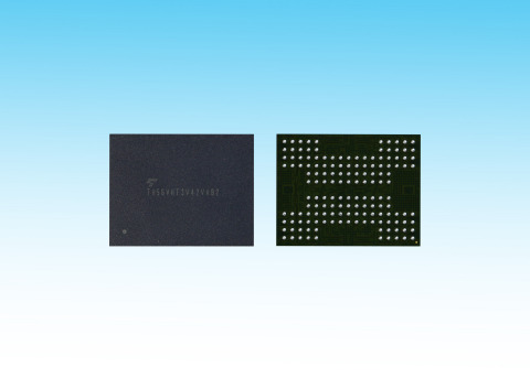
The device with TSV technology applied features a structure that performs high-speed data I/O while reducing power consumption, with vertical electrodes and bias passing through the silicon die to provide connectivity. The actual performance in use has already been demonstrated through Toshiba's previously announced 2D NAND flash memory.
Toshiba Memory Corporation combined the 48-layer 3D flash process with TSV technology to successfully increase the product's programming bandwidth while lowering power consumption. The company explained that the power efficiency of a single package is approximately twice that of the same-generation BiCS FLASH™ memory using wire bonding technology. Additionally, the company stated that BiCS FLASH memory with TSV technology applied has a structure with 16 dies stacked in a single package, achieving a capacity of 1 terabyte (TB).
The company plans to commercialize BiCS FLASH memory with TSV technology applied and provide solutions suitable for storage applications requiring low latency and high bandwidth IOPS (input/output operations per second)/watt, including high-performance enterprise SSDs.
관련뉴스
Toshiba Expands Lineup of Embedded NAND Flash Memory for Automotive Applications
Toshiba Corporation's Storage & Device Solutions Company has announced the launch of embedded NAND flash memory products that comply with JEDEC e·MMC™ version 5.1 and meet the AEC-Q100 Grade 2 specification.
2017.01.02by 홍보라 기자
Toshiba Launches Enterprise-Class 2.5-inch HDD
Toshiba has launched the AL14SX series with enterprise-grade performance for critical server and storage applications. Toshiba Corporation's Storage and Electronic Devices Solution Company announced that it has added a new product to its hard disk drive (HDD) lineup with enterprise-grade performance for critical server and storage applications.
2017.06.14by 신윤오 기자
Toshiba Begins Mass Production of Graphics Processors for Wearables and IoT
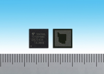
Toshiba Electronic Devices & Storage Corporation has announced the beginning of mass production of the TZ1201XBG ApP Lite™ processor product family for Internet of Things (IoT) devices, including wearable products. The compact TZ1201XBG graphics processor is based on a high-performance 32-bit ARM Cortex-M4F processor capable of operating at 96MHz (up to 120MHz during overclocking). The combination of the ARM core and on-chip power management provides the TZ1201XBG with low power consumption of 70μA/MHz in active mode. With a 350mAh battery and always-on display, the second-hand clock application can operate for approximately one month per charge, while the minute-hand clock can operate for approximately two months.
2017.07.11by 신윤오 기자

Intel Unveils Next-Generation 'Core Ultra Series 3' and vPro Platform for Enterprise PCs
Intel has officially unveiled the "Intel Core Ultra Series 3" for next-generation enterprise PCs and the latest vPro platform, addressing a wide range of demands from enterprise notebooks to high-performance workstations.
2026.03.26by 배종인 기자

ROHM Launches ESD Protection Diode Compatible with High-Speed Interfaces of 10Gbps or Higher
Semiconductor specialist ROHM has developed the 'RESDxVx series' of ESD (electrostatic discharge) protection diodes capable of responding to next-generation high-speed data communication environments exceeding 10Gbps, simultaneously enhancing both signal quality maintenance required in high-speed interfaces and IC protection performance.
2026.03.26by 배종인 기자











