



OnSemiconductor unveils CMOS sensor platform to elevate image quality in autonomous vehicles
 Published2017.10.26 15:10
OnSemiconductor has introduced a CMOS image sensor platform that delivers a new level of performance and image quality for automotive applications such as ADAS, mirror replacement, rear and surround view systems, and autonomous driving.
The Hayabusa platform features a groundbreaking 3.0-micron backside-illuminated pixel design that provides the industry's highest 100,000 electrons of full-well capacity. Key features of this device include LED flicker mitigation (LFM) and on-chip HDR, as well as real-time functional safety and automotive grade qualification.
Ross Jatou, Vice President and General Manager of OnSemiconductor's Automotive Solutions division, stated: "The Hayabusa product family enables automotive manufacturers to meet evolving ADAS standards such as Euro NCAP 2020 and provides next-generation capabilities including electronic mirrors, high-resolution surround view systems, and anti-flicker technology. The scalable sensor with optical sizes ranging from 1/2" to 1/4" can be applied across multiple types of automotive platforms, allowing customers to reduce development time and effort while shortening time-to-market."
He added: "OnSemiconductor has been supplying image sensors with this pixel architecture for high-end digital cameras used in cinema and television production. We have applied this proven architecture to new sensors developed from the ground up for automotive standards."
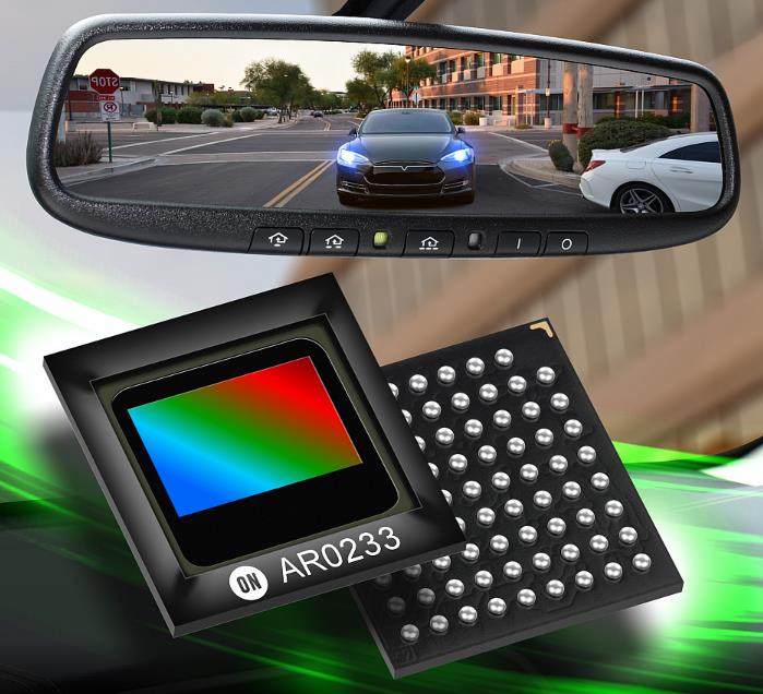
The high full-well capacity of this pixel design enables the Super-Exposure function, which allows all Hayabusa family devices to provide 120dB HDR imaging with LFM for high image fidelity in the most challenging scenes without sacrificing low-light sensitivity. The simultaneous HDR and LFM capabilities represent a critical function that enhances safety by identifying all objects and potential hazards in both very dark and very bright areas of a scene.
The platform's LFM function across various LEDs, from front and rear lights to traffic signals, effectively prevents flicker from pulsed light sources that could distract the driver or cause misinterpretation by machine vision algorithms in forward-facing ADAS scenarios.
The Hayabusa product family also features safety capabilities that comply with ISO26262 requirements in real-time, enabling the sensor to immediately alert the system processor if any issues or potential errors occur. These features enable system designs rated up to ASIL-C. Real-time functionality allows immediate identification of errors instead of transmitting the entire image to the processor and waiting for image analysis.
The faster response time enables the system processor to take immediate corrective action to address issues. This capability is critical given that vehicles traveling on highways easily cover 100 feet in less than one second.
Related news
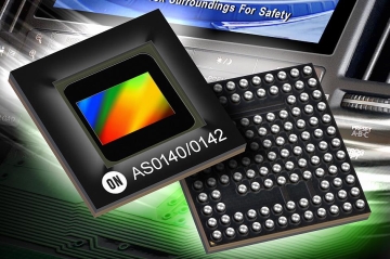
onsemi Launches High-Integration Sensing Products in Automotive Imaging Field
onsemi continues to advance its technology in the rapidly growing automotive imaging field with the introduction of two new high-integration 1.0 megapixel (Mp) CMOS image sensing products. These devices provide a complete solution featuring image sensor and processing functions integrated into a low-power SoC that simplifies and accelerates adoption in applications such as rear and surround-view cameras. Compared to conventional solutions consisting of discrete sensor and processor components, these devices enable over 30% superior PCB space savings, allowing designers to implement camera solutions without affecting vehicle styling or aesthetics.
2017.10.11by 김지혜 기자

ON Semiconductor Expands Partnership with Fujitsu Semiconductor to Drive 8-inch Fab Growth
Fujitsu Semiconductor and ON Semiconductor announced that they have agreed for ON Semiconductor to acquire an additional 30% incremental stake in Fujitsu's 8-inch wafer fab line located in Izu-Wakamatsu, resulting in ON Semiconductor holding a 40% ownership stake. Under the agreement between the two companies executed in 2014, ON Semiconductor owned a 10% stake in Fujitsu's Izu 8-inch fab. The initial transfer commenced in 2014, and successful wafer production and semiconductor mass production began from June 2015. As ON Semiconductor has continued to increase production volume at the Izu 8-inch fab, both companies determined that they would maximize mutual business value through future strategic partnership. ON Semiconductor plans to increase its ownership stake to 60% by the second half of 2018 and further expand it to 100% in the first half of 2020, thereby raising its global market share. Through this expanded production capacity, ON Semiconductor will further expand its business in accordance with industry demand, thereby improving supply chain flexibility.
2017.10.12by 김지혜 기자
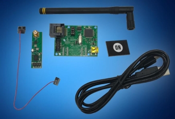
Mouser Electronics Launches Sigfox Connectivity Solutions from ON Semiconductor for Low-Power IoT Networks
Mouser Electronics is now distributing Sigfox connectivity solutions from ON Semiconductor. ON Semiconductor's Sigfox-compliant product family provides a range of hardware and software development tools that simplify the design of new IoT (Internet of Things) applications. The ON Semiconductor Sigfox portfolio available through Mouser offers ultra-low-power connectivity devices and development kits to meet the demand for IoT devices that transmit small amounts of data. The AX-SFxx and AX-SFxx-API RF transceivers serve as single-chip solutions for nodes on the Sigfox network, featuring both uplink and downlink functionality.
2017.10.23by 김지혜 기자

A single misaligned light means 'defect'… Vehicle interior lighting now guarded by semiconductors and software
Automotive interior lighting is moving beyond its role as 'auxiliary lighting.' As it becomes a core element of user experience (UX) that expresses brand identity through color and animation while reflecting driver preferences, the LED interior ambient lighting market is growing rapidly. In connection with this, we met in advance with Choi Young-jae, Research Director at Dabo Corporation, who will present a technical webinar session on "Intelligent LED Interior Lighting Solutions Illuminating Future Vehicles," to hear about market trends and changes in design requirements.
2026.08.28by 명세환 기자

TI Unveils Multi-Axis Coreless Current Sensor TMCS2100-Q1 for HEV/EV Traction Inverters
Texas Instruments has unveiled the TMCS2100-Q1, a multi-axis coreless Hall-effect current sensor for HEV and EV traction inverters. By simultaneously measuring horizontal and vertical magnetic fields through multi-axis sensing technology, it achieves up to 20 times higher accuracy compared to conventional single-axis sensors, while the busbar-unmodified design provides mechanical design flexibility. It simultaneously meets the high-accuracy requirements and miniaturization driven by the expansion of 800V architectures.
2026.08.27by 배종인 기자











