


Samsung Electronics begins mass production of 10nm 2nd generation SoC products
 Published2017.11.29 11:04
Samsung Electronics announced that it will begin mass production of SoC (System on Chip) products based on the 10nm 2nd generation FinFET process (10LPP, Low Power Plus).
This 10nm 2nd generation process has improved performance and power efficiency by 10% and 15%, respectively, compared to the existing 1st generation process (10LPE, Low Power Early). In addition, since the 10LPP process is based on the 1st generation process that has already been verified through mass production, the time from product development to mass production (TAT, turn-around time) is significantly reduced, and it has the advantage of making it easy to secure initial yields.

Products using Samsung Electronics' 10LPP process are expected to be applied to a wider range of customers and applications, starting with new IT products to be released early next year.
“The 10LPP process not only provides customers with improved performance, but also enables customers to launch new products in a timely manner through high initial yields,” said Sang-Hyun Lee, senior vice president of Samsung Electronics’ foundry marketing team. “Samsung Electronics’ long-term 10nm utilization strategy will continue by expanding the 10nm-based process to the 8LPP process to provide differentiated competitiveness in various applications in the future.”
Samsung Electronics announced that it has completed preparations for mass production of the S3 line foundry process located at the Hwaseong Campus along with mass production of the 10nm second-generation process. The S3 line is the third foundry fab, following the S1 line in Giheung Campus and the S2 line in Austin, Texas, where not only the 10nm process but also Samsung's 7nm FinFET process using EUV technology will be mass-produced.
관련뉴스
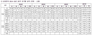
Samsung Electronics Reports Record Quarterly Earnings in Q3 2017
삼성전자는 2017년 3분기 실적이 매출 62.05조원, 영업이익 14.53조원이라고 발표했다. 매출과 영업이익 모두 분기사상 최대 실적이다. 3분기 매출은 메모리 시장의 호황 지속과 플렉서블 OLED 패널 판매 확대로 전년 동기 대비 약 30% 증가했고, 영업이익도 반도체 사업 수익성이 개선되고, 스마트폰 판매도 회복되면서 전년 동기 대비 9.3조원 증가했다. 전분기 대비 매출은 2%, 영업이익은 0.47조원 증가했다. 부품 사업은 메모리 가격 강세, 고부가LSI 제품 판매 확대로 실적이 대폭 개선됐으나, 디스플레이의 경우 플렉서블 OLED 패널 판매 확대에도 불구하고 신규라인 초기 가동(Ramp-up) 비용 증가 등으로 실적이 전분기 대비 둔화됐다.
2017.10.31by 김지혜 기자

Samsung Electronics and Qualcomm Begin Mass Production of Server Processors Based on 10nm Process
퀄컴(Qualcomm)이 미국 산호세에서 세계 최초 10나노 공정 기반의 서버 프로세서 'Centriq 2400'를 출시하고 삼성전자를 통해 양산을 시작한다고 발표했다. 삼성전자와 퀄컴은 오랜 기간 동안 파운드리 분야에서 전략적 협력 관계를 유지해 왔으며 최근 14나노와 10나노 등 첨단 공정을 적용한 모바일 프로세서 양산에 이어 서버용 프로세서로까지 영역을 확대했다.
2017.11.09by 김지혜 기자
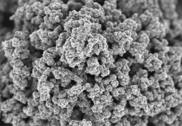
Samsung Electronics Secures Core Battery Technology Five Times Faster than Lithium-ion Batteries
삼성전자 종합기술원(손인혁?두석광 연구팀)이 기존 리튬이온전지보다 충전용량은 45% 향상시키면서 충전속도를 5배 이상 빠르게 만들 수 있는 배터리 소재 ‘그래핀 볼’ 개발에 성공했다. 기존 배터리는 고속충전 기술을 사용하더라도 완전충전에 1시간 가까이 걸렸지만, ‘그래핀 볼’ 소재를 사용한 배터리는 12분이면 완전히 충전할 수 있다. 또한 전기차용 배터리가 요구하는 온도 기준인 60 ℃까지 안정성을 유지할 수 있다. 이와 관련한 연구성과는 최근 과학저널 ‘네이처 커뮤니케이션즈’(Nature Communications) 온라인에 <그래핀 볼을 이용한 고속충전 및 고용량 리튬이온전지 구현>이라는 제목으로 게재됐다.
2017.11.27by 김지혜 기자

Intel Unveils Next-Generation 'Core Ultra Series 3' and vPro Platform for Enterprise PCs
인텔이 차세대 기업용 PC를 위한 ‘인텔 코어 Ultra 시리즈 3’와 최신 vPro 플랫폼을 공식 발표하며, 기업용 노트북부터 고성능 워크스테이션까지 폭넓은 수요 충족에 나섰다.
2026.03.26by 배종인 기자

ROHM Launches ESD Protection Diode Compatible with High-Speed Interfaces of 10Gbps or Higher
반도체 전문 기업 로옴(ROHM)이 10Gbps를 넘어서는 차세대 고속 데이터 통신 환경에 대응할 수 있는 ESD(정전기 방전) 보호 다이오드 ‘RESDxVx 시리즈’를 개발하며, 고속 인터페이스에서 요구되는 신호 품질 유지와 IC 보호 성능을 동시에 끌어올렸다.
2026.03.26by 배종인 기자











