



Samsung Electronics Begins Full-Scale Mass Production of '2nd Generation 10nm-Class (1y Nano) DRAM'
 Published2017.12.20 11:46
Samsung Electronics has overcome the greatest process development challenges in history and is mass-producing '10-nanometer class 2nd generation (1y nanometer) DRAM'.
Samsung Electronics has been mass-producing the world's smallest chip size 10-nanometer class 8Gb DDR4 (Double Data Rate 4) DRAM since last month.
Samsung Electronics, which ushered in the era of 10-nanometer class DRAM by mass-producing '1x-nanometer (1st generation 10-nanometer class) 8Gb DRAM' in February 2016, has overcome the limitations of semiconductor microfabrication in 21 months.
Samsung Electronics has built a competitive edge that enables it to respond in a timely manner to the increasing demand for premium DRAM from global customers by increasing productivity by approximately 30% compared to first-generation 10-nanometer class DRAM without using next-generation extreme ultraviolet (EUV) lithography equipment.
Samsung Electronics plans to enter a full-scale 10-nanometer DRAM mass production system, excluding some application products, through the mass production of this second-generation 10-nanometer DRAM, which doubles the capacity, speed, and power consumption efficiency of the 2y-nanometer (20-nanometer class) 4Gb DDR3 produced in 2012.
Meanwhile, three advanced innovative processes have been applied to this second-generation 10-nanometer class DRAM product: ① 'ultra-high speed/ultra-low power/ultra-small circuit design', ② 'ultra-high sensitivity cell data sensing system design', and ③ 'second-generation Air Gap process'.
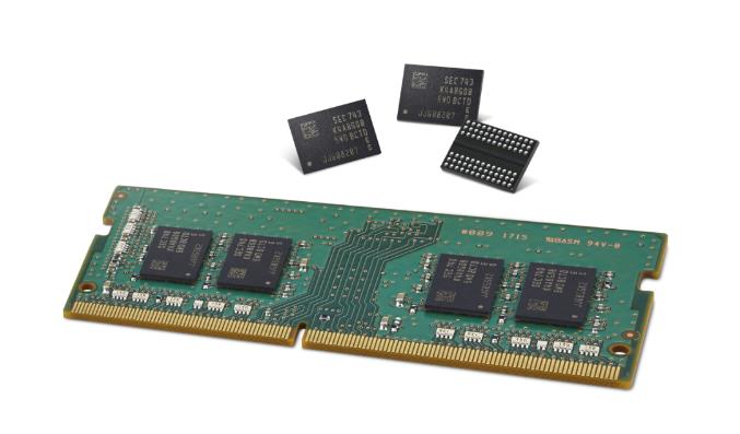
The second-generation 10nm-class DRAM is based on ① 'ultra-high speed/ultra-low power/ultra-small circuit design'Compared to the first generation 10nm-class DRAM, speed has improved by more than 10% and power consumption has been reduced by more than 15%.
② The 'ultra-high sensitivity cell data sensing system design' technology is a technology that improves cell data reading characteristics by more than double by more precisely verifying data stored in the cell through the development of an ultra-precision voltage difference detection system.
③ The '2nd generation Air Gap process' is a process technology that fills the micro-region around a bit line through which current flows with air, which has excellent insulating properties, instead of a specific material.
This technology enables the development of ultra-high sensitivity cells by minimizing the amount of unnecessary charge generated around the bitline, and can significantly reduce the chip size by improving the integration density of the cell array.
Based on these advanced innovative process technologies, Samsung Electronics has secured the industry's first mass production base for next-generation premium DRAM, including DDR5 for servers, LPDDR5 for mobile devices, HBM3 for supercomputers, and GDDR6 for ultra-high-speed graphics.
"We have broken through the limits of semiconductor miniaturization technology through the development of innovative technology based on a paradigm shift," said Jin Gyo-young, President of Samsung Electronics' Memory Business Division. "We will further strengthen our competitive edge by transitioning the premium DRAM market to the 10-nanometer class through the expansion of 1y-nanometer DRAM production."
Comments
Related news
Samsung Electronics Expands Premium Market Through Mass Production of D-RAM for AI Systems
Samsung Electronics is rapidly increasing production volumes of 8GB High Bandwidth Memory (HBM2) D-RAM, expanding supply not only to the supercomputer (HPC) market but also to network and graphics card markets. Samsung Electronics began mass production of 8GB HBM2 D-RAM in June of last year, pioneering the memory market for supercomputers utilized in artificial intelligence (AI) services, and has subsequently expanded the application scope of premium D-RAM to the existing high-end graphics card market.
2017.07.19by 김자영 기자

Samsung Electronics Sees Q2 Earnings Soar on Increased Galaxy S8 Sales and Semiconductor Boom
Samsung Electronics announced its second quarter 2017 results on a consolidated basis, with sales of 61 trillion won and operating profit of 14.07 trillion won. Second quarter results showed sales reaching 61 trillion won, up 20% year-over-year, driven by continued favorable memory market conditions and expanded global sales of the Galaxy S8 and S8+. Operating profit also achieved 14.07 trillion won, up 5.92 trillion won year-over-year, with an operating margin of 23.1%, as component business profits increased significantly. The component business performance improved substantially due to strong memory prices, expanded sales of high-capacity server DRAM and SSDs, and increased sales of Galaxy S8 components from the System LSI and display businesses. In the second quarter, the semiconductor business achieved sales of 17.58 trillion won and operating profit of 8.03 trillion won.
2017.07.27by 신윤오 기자
The CPU era is over, and the 'memory-centric computing' era is here
This year, memory has led the boom in the global semiconductor market. Memory experienced a surge because supply failed to keep up with demand, causing memory prices to rise. So what changes will the memory market face as the artificial intelligence (AI) era approaches? Doh Hyun-woo, senior research fellow at Mirae Asset Daewoo, stated: "We expect conditions to remain favorable through the first half of next year. DRAM will continue its upward price trend thanks to restrained capacity investment and server-type demand. NAND has started experiencing price increases due to iPhone X demand. Memory supply and demand are expected to remain balanced through the first half of 2018." He added: "In the fourth quarter of next year, Chinese memory semiconductor companies are scheduled to begin production on a small scale, which could be a variable factor." As memory semiconductor demand is expected to remain favorable, what issues should we pay attention to? The research fellow emphasized that memory-centric computing warrants close attention.
2017.10.23by 김지혜 기자

Intel Unveils Next-Generation 'Core Ultra Series 3' and vPro Platform for Enterprise PCs
Intel has officially unveiled the "Intel Core Ultra Series 3" for next-generation enterprise PCs and the latest vPro platform, addressing a wide range of demands from enterprise notebooks to high-performance workstations.
2026.03.26by 배종인 기자

ROHM Launches ESD Protection Diode Compatible with High-Speed Interfaces of 10Gbps or Higher
Semiconductor specialist ROHM has developed the 'RESDxVx series' of ESD (electrostatic discharge) protection diodes capable of responding to next-generation high-speed data communication environments exceeding 10Gbps, simultaneously enhancing both signal quality maintenance required in high-speed interfaces and IC protection performance.
2026.03.26by 배종인 기자











