기사입력 2025.03.31 15:14
.jpg)
UNIST(총장 박종래) 전기전자공학과 변영재 교수팀이 3차원 공간 어디에서든 충전이 가능한 전기공진 방식의 무선전력전송(ERWPT) 기술을 세계 최초로 개발하며, 벽, 바닥, 공중 등 3차원 공간 안에서 어디서든 충전이 가능해 향후 가정에서 뿐만 아니라 스마트로봇 등 산업에서도 다양하게 사용될 것으로 기대가 모아진다.
2024-12-12 오전 8:46:56by 배종인 기자
UNIST(총장 박종래) 지구환경도시건설공학과 임정호 교수팀이 1년 뒤의 북극 해빙 농도를 6% 이내 오차 정확도로 예측할 수 있는 인공지능 모델을 개발하며, 북극 해빙 변화에 대한 중장기 예측 정보 제공이 가능해져 북극 항로 개발, 해양 자원 탐사 등에 도움이 될 전망이다.
2024-12-26 오전 9:06:48by 배종인 기자
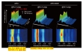
UNIST(총장 박종래) 화학과 권오훈 교수팀이 투과전자현미경 안에서 미세시료의 온도를 정밀하게 측정할 수 있는 범용 ‘나노온도계’를 개발했다.
2025-01-02 오후 3:45:14by 배종인 기자
UNIST(총장 박종래) 화학과 민두영·권태혁·민승규 교수팀은 청색광(블루라이트; blue light)에 의해 세포 단백질이 손상되는 새로운 경로를 규명했다고 6일 밝혔다.
2025-01-06 오전 10:25:10by 배종인 기자

UNIST 화학과 오현철 교수팀과 서울대학교 화학부 이은성 교수팀은 이온교환 방식을 통해 다공성 물질인 금속 유기 골격체(MOF)의 기공을 0.01 나노미터 단위까지 조절할 수 있는 기술을 개발하며, 자연계 전체 수소 중 0.015%만 존재하는 중수소(D2)를 효율적으로 분리할 수 있게 됐다.
2025-02-12 오후 2:15:13by 배종인 기자
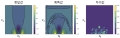
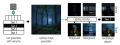
UNIST 원자력공학과 이지민·윤의성 교수팀이 플라즈마 상태를 설명하는 수학 방정식의 해를 가속화 해 구할 수 있는 딥러닝 기반 인공지능 모델 ‘FPL-net’을 개발하며, 핵융합로 안의 플라즈마 상태를 기존보다 1,000배 빠르게 시뮬레이션할 수 있을 것으로 기대된다.
2025-02-17 오전 8:19:57by 배종인 기자
UNIST 인공지능대학원 백승렬 교수팀이 창의적인 텍스트 프롬프트 기반의 조명 효과를 적용하는 인공지능 모델 ‘텍스트투리라이트(Text2Relight)’를 개발하며, 복잡한 편집도구를 쓰지 않고도 텍스트 입력만으로 ‘따끈따끈한 치킨’, ‘차가운 푸른빛’과 같은 언어의 감성까지 담아 사진이나 영상의 색감을 쉽게 보정할 수 있게 됐다.
2025-02-26 오후 4:15:46by 배종인 기자
.jpg)
UNIST 박승배 교수가 현대 과학 이론과 철학적 질문을 쉽게 풀어낸 과학철학 개론서 ‘Reflections upon Science’를 출간했다.
2025-02-28 오후 2:33:07by 배종인 기자
UNIST는 에너지화학공학과 이현욱 교수팀이 배터리 양극 신소재인 과리튬 소재의 산소 발생 원인을 규명하고 이를 해결할 소재 설계 원리를 제시하며, 향후 장거리 주행 배터리 개발이 가시화 될 것으로 기대된다.
2025-03-18 오전 9:00:48by 배종인 기자

UNIST 신소재공학과 조승호·송명훈 교수 연구팀은 태양광 전기를 활용하여 이산화탄소 배출 없이 암모니아를 합성하고, 동시에 폐플라스틱에서 고부가가치 물질인 글리콜산을 생산하는 새로운 광전기화학 시스템을 개발했다.
2025-03-28 오후 3:40:45by 배종인 기자

[열린보도원칙] 당 매체는 독자와 취재원 등 뉴스이용자의 권리 보장을 위해 반론이나 정정보도, 추후보도를 요청할 수 있는 창구를 열어두고 있음을 알려드립니다.
고충처리인 장은성 070-4699-5321 , news@e4ds.com