


Samsung Electronics ships eMRAM based on 28nm FD-SOI process
 Published2019.03.06 11:01
| Achieves chip miniaturization by embedding MRAM in SoC
| Simple design structure significantly reduces production costs
Samsung Electronics on the 6th shipped eMRAM (embedded MRAM) solution products based on 28nm FD-SOI process.
FD-SOI (Fully Depleted-Silicon on Insulator) process is a process that can reduce leakage current by coating an insulating layer over a silicon wafer.
MRAM (Magnetic Random Access Memory) is a memory semiconductor with the characteristic of being non-volatile (data is retained even when power is off) while having speed comparable to DRAM. With these two technologies combined, a next-generation embedded memory has been created that consumes less power, has very fast speed, is easy to miniaturize, and is also inexpensive.
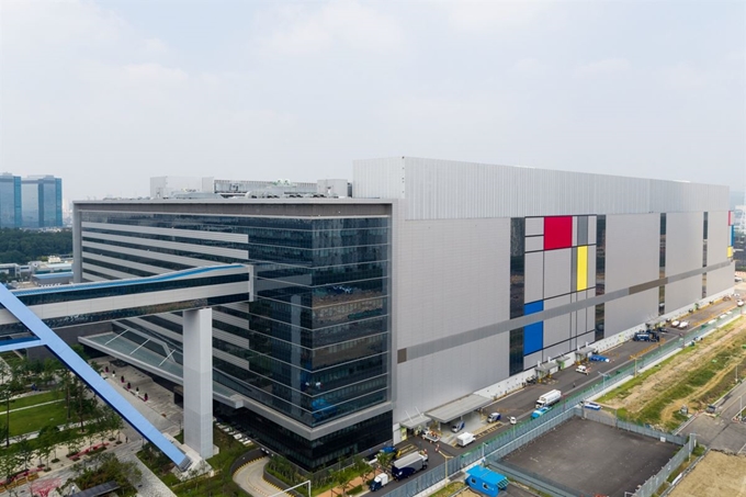
Samsung Electronics Foundry production line
Samsung Electronics' Foundry Business Division has strengthened its technology leadership in the foundry field by combining this product with SoC.
Embedded memory is a memory module that plays a role in information storage in system semiconductors such as MCU or SoC used in small electronic products like IoT devices. Primarily eFlash (embedded Flash Memory) based on flash technology is used.
However, eFlash has disadvantages in terms of speed and power efficiency because it goes through a process of deleting existing data that was previously stored when recording data.
Samsung Electronics' eMRAM solution based on 28nm FD-SOI process does not require deletion when recording data, and implements write speed approximately 1000 times faster than existing eFlash.
It also has non-volatile characteristics, maintaining stored data in a power-off state without consuming standby power, and the operating voltage required for data recording is also lower, providing good power efficiency.
Samsung Electronics' eMRAM solution has a simple structure, so it can be implemented by adding only minimal layers to existing logic process-based designs, thereby reducing design burden for customers and lowering production costs.
Meanwhile, Samsung Electronics will hold an event on the 6th at Giheung Campus to commemorate the first shipment of mass-produced eMRAM products based on 28nm FD-SOI process.
Samsung Electronics' strategy is to continuously expand embedded memory solutions by starting 1Gb eMRAM test chip production within this year, thereby securing differentiated foundry competitiveness.
Sang-hyun Lee, Executive Director of Strategic Marketing Team at Samsung Electronics Foundry Business Division, stated, "We have overcome difficulties in utilizing new materials and have presented a next-generation embedded memory solution," and added, "By expanding eMRAM application to Samsung's verified foundry logic process and providing differentiated competitiveness and excellent productivity, we will respond to customer and market demands."
Comments
Related news
Evolving Foundry Technology Leads the 4th Industrial Revolution
Samsung Electronics Foundry Division President Jung Eun-seung delivered a keynote speech at the International Electron Devices Meeting held in San Francisco on the theme of "Industry 4.0 and Foundry." In his keynote address, President Jung emphasized that to process the rapidly growing data in the Industry 4.0 era, semiconductor integration density must be increased to continuously improve performance and power efficiency. He stressed that the evolution of advanced foundry technologies such as EUV lithography and STT-MRAM is critical for this. He also noted that implementing new ideas such as autonomous vehicles and smart homes requires advanced semiconductor technology. Going forward, the foundry business will not only strengthen its existing role in contract semiconductor manufacturing but will also expand collaboration ranging from design services to package and test operations according to customer requests.
2018.12.04by 이수민 기자
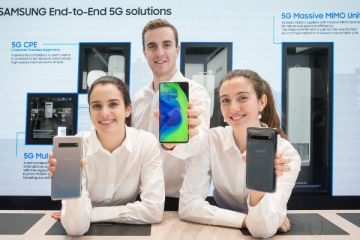
[5G! MWC19] Samsung Electronics Showcases 5G Commercial Technology, From Smartphones to Communications Equipment
Samsung Electronics will showcase an integrated 5G solution spanning from chipsets to smartphones and telecommunications equipment at MWC19, demonstrating its commercial 5G technological capabilities. Using Samsung Electronics' first 5G smartphone, Galaxy S10 5G, and telecommunications equipment currently providing commercial services in the United States and Korea, visitors will be able to directly experience 5G's ultra-high-speed data transmission, ultra-low latency, and ultra-connectivity. Through this, Samsung demonstrated that 5G wireless communication is not a future technology but an already present reality, and showcased the potential to provide unprecedented experiences not only in smartphones but also in diverse fields such as connected cars and smart factories.
2019.02.25by 이수민 기자
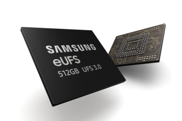
Samsung Electronics begins mass production of 512GB eUFS 3.0, promising mobile devices faster than laptops.
Samsung Electronics has begun mass production of 512GB eUFS 3.0, the next-generation mobile memory, securing a leading position in the premium smartphone memory market. The eUFS 3.0 product achieves sequential read speeds of 2100MB/s, more than twice faster than the existing eUFS 2.1. Samsung Electronics explained that through this product, which features NVMe SSD-level performance, consumers can experience ultra-slim notebook-level performance even on next-generation mobile devices with ultra-high resolution.
2019.02.28by 이수민 기자

Intel Unveils Next-Generation 'Core Ultra Series 3' and vPro Platform for Enterprise PCs
Intel has officially unveiled the "Intel Core Ultra Series 3" for next-generation enterprise PCs and the latest vPro platform, addressing a wide range of demands from enterprise notebooks to high-performance workstations.
2026.03.26by 배종인 기자

ROHM Launches ESD Protection Diode Compatible with High-Speed Interfaces of 10Gbps or Higher
Semiconductor specialist ROHM has developed the 'RESDxVx series' of ESD (electrostatic discharge) protection diodes capable of responding to next-generation high-speed data communication environments exceeding 10Gbps, simultaneously enhancing both signal quality maintenance required in high-speed interfaces and IC protection performance.
2026.03.26by 배종인 기자











