



Samsung Electronics Reveals Plans for Mass Production of Baidu's High-Performance AI Chips
 Published2019.12.18 17:15
Comprehensive foundry solutions covering design, process, and packaging
Samsung Electronics announced that it plans to mass-produce the 'Kunlun' AI chip, based on the 14nm process of Baidu, a major Chinese internet search engine company, in early 2020.
(1).jpg)
▲ Baidu's AI chip KUNLUN <Image=Samsung Electronics>
With this first foundry collaboration, Samsung Electronics is now able to expand its foundry business scope to include AI chips that can be used in cloud and edge computing.
Baidu's Kunlun is an artificial intelligence chip that can be used in various fields of AI ranging from cloud to edge computing. It is a product realized with high performance of 512 GBps bandwidth and 260 TOPS (Tera Operations Per Second, 150W) by applying Baidu's proprietary XPU architecture, Samsung Electronics' 14nm process, and I Cube (Interposer Cube) packaging technology.
Samsung Electronics has improved power (PI) and electrical signal (SI) quality by more than 50% compared to existing solutions by applying a foundry solution optimized for High Performance Computing (HPC).
This improves the noise generated when a signal is transmitted to the chip, and the voltage It is a solution that maintains a constant level to enable the circuit to operate more stably.
I Cube is Samsung Electronics' unique differentiated 2.5D packaging technology that integrates SoC chips and HBM (High Bandwidth Memory) chips onto a silicon interposer (Si-Interposer). This technology has the advantage of increasing transfer speeds and reducing package area by placing each chip within a single package.
Ouyang Jian, Chief Architect and Head of AI Semiconductor Development at Baidu, stated, “We are pleased to lead the HPC industry with the successful development of Kunlun. Kunlun was a challenging project aiming for high performance and reliability, and we were able to achieve the desired results through Samsung’s HPC foundry solutions.”
Lee Sang-hyun, Senior Vice President of the Marketing Team at Samsung Electronics’ DS Division Foundry Business Unit, said, “Starting with mobile products, we have now expanded our foundry scope to the HPC field,” adding, “In the future, we will continue to provide comprehensive foundry solutions, including design support through the ecosystem, 5/4 nanometer advanced processes, and next-generation packaging technology.”
Comments
Related news
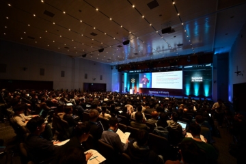
Samsung Electronics "Will Be Reborn as an Innovation Company in the AI Field"
At the Samsung AI Forum 2019, Koh Dong-jin, President and CEO, stated in his opening remarks, "In the hyper-connected era driven by 5G, AI, and IoT technologies, companies that innovate user experience will become global business winners," and added, "Samsung Electronics will be a company that leads the future at the forefront of 5G and AI innovation."
2019.11.11by 최인영 기자
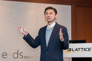
Lattice Nexus, Low-Power FPGA Platform for Edge AI Unveiled
Lattice Semiconductor announced Nexus, a new low-power FPGA platform, and CrossLink-NX, the first device based on it. The Lattice Nexus platform was designed for embedded developers looking to implement AI applications at the edge, and was developed using Samsung Electronics' 28nm FD-SOI process technology.
2019.12.11by 이수민 기자
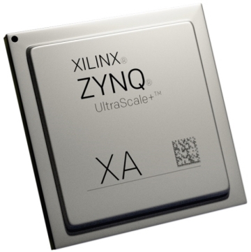
Xilinx Solution Adopted in Baidu ACU
Xilinx's automotive-grade Zynq UltraScale+ MPSoC is being applied to Baidu's production-ready ACU advanced platform for automated valet parking systems. For specific scenarios and functional verification of automated valet parking that require deep learning inference capable of processing complex driving environments, sensor fusion and AI processing capabilities are enabled through the XA Zynq UltraScale+ MPSoC.
2019.12.19by 최인영 기자
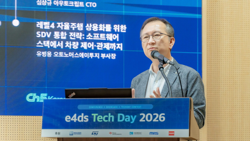
[e4ds Tech Day 2026 ⑨] Sim Sang-gyu, Autocrypt CTO: "In the Physical AI Era, Automotive Security Must Extend Beyond the Vehicle"
At e4ds Tech Day 2026, Sim Sang-gyu, CTO of Autocrypt, explained automotive cybersecurity strategies in the era of Physical AI and SDV (Software-Defined Vehicle). Automobiles are evolving as part of an ecosystem connected to AI, cloud, chargers, IoT, and robots, and he emphasized that the scope of security must expand beyond the vehicle interior to the entire connected environment. In particular, AI model tampering, adversarial attacks, OTA updates, and EV charger hacking were identified as major threats. He explained that response measures require zero trust, AI model integrity protection, intrusion detection, Security by Design and Default, and full lifecycle security management, and that proactive security system establishment beyond regulatory compliance is critical for securing future mobility competitiveness.
2026.10.12by 배종인 기자
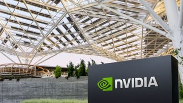
NVIDIA to Invest $1 Billion in U.S. Science Over Next Five Years
NVIDIA has announced plans to invest $1 billion over the next five years to strengthen U.S. scientific and technological competitiveness. The company will enhance cutting-edge artificial intelligence research and development capabilities in key areas including quantum computing, healthcare, and energy security, while expanding support for higher education research institutions and cloud service providers. NVIDIA is participating as a major industry partner in the White House Office of Science and Technology Policy's Genesis Mission, and is promoting supercomputer construction in collaboration with national laboratories including Argonne and Los Alamos.
2026.10.12by 배종인 기자











