


EUV, the Next-Generation Semiconductor Process, "Will It Survive Moore's Law?"
 Published2020.11.19 12:15
EUV process requires power source and causes severe metal contamination
Parallel use with DPT/QPT processes below 5nm
Moore's Law states that semiconductor chip performance doubles every 18 months. This law, proposed by Intel co-founder Gordon Moore in 1965, has been the basis for semiconductor companies' manufacturing strategies.
However, since the 2010s, the increasing difficulty of process miniaturization has slowed the improvement in semiconductor chip performance, raising many questions about Moore's Law. However, with the full-scale adoption of extreme ultraviolet (EUV) lithography in semiconductor manufacturing, Moore's Law is expected to be extended.
According to the Korea Semiconductor Industry Association (KSIA), the wavelength of EUV is 13.5 nm, which is much shorter than the 193 nm of argon fluoride (ArF), which has been widely used so far, and can increase the precision of semiconductor exposure processes.
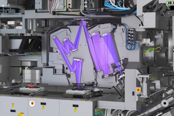
The EUV process, which is attracting attention as a method for realizing next-generation semiconductor microfabrication, is currently being applied mainly in logic and foundry processes. In both fields, it is more cost-effective to use the EUV process than the DPT (Double Patterning Technology)/QPT (Quadruple Patterning Technology) process at 7nm or below.
However, the industry predicts that rather than solely relying on EUV technology to achieve cost competitiveness, EUV technology will likely be responsible for some microfabrication processes. EUV is extremely difficult to implement, requiring separate power plants for power, and is also prone to metal contamination.
Currently, the industry largely relies on existing ArF immersion equipment to implement fine patterns. ArF immersion can theoretically be used up to the 40nm process. For processes below 30nm, the DPT process is used in addition to ArF immersion equipment.
EUV technology enables 7nm and 5nm processes without repeating the exposure process. The challenge lies in mass production. Therefore, technology development is expected to focus on using EUV locally in areas requiring fine patterns, while utilizing conventional immersion processes for other areas.
Furthermore, implementing EUV for processes below 5nm will require the introduction of a DPT process alongside EUV. Therefore, for processes below 5nm, it seems likely that DPT and QPT processes will need to be utilized alongside EUV.
It is expected that future exposure processes will be developed by combining various technologies rather than applying a single technology. Process refinement is expected to continue through EUV technology and the development of alternative technologies, including DPT and QPT, which are existing exposure repetitive processes.
◇ The introduction of EUV will also change semiconductor structures and materials.
In the logic and foundry fields, EUV is being introduced after 7nm, and 3D structure technology development is also progressing in parallel.
Up to the 5nm or 4nm process, EUV will be used exclusively, but below 5nm, DPT or QPT technology will be applied to EUV technology, and the structure is also expected to change to the GAA (Gate-All-Around) method that surpasses FinFET.
In the DRAM field, EUV technology will be introduced in earnest after 1zm, and diversification of material technologies such as hafnium oxide (HfO2) in the cap process is expected.
Comments
Related news
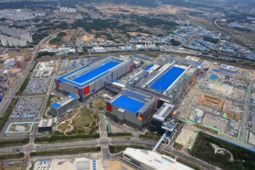
Samsung Electronics to Build 5nm EUV Foundry Production Line in Pyeongtaek
Samsung Electronics announced that it will establish a foundry production facility at its Pyeongtaek campus in Gyeonggi Province to respond to demand for EUV-based products. Samsung Electronics has commenced construction of the Pyeongtaek foundry line this month, with plans to begin full-scale mass production of 5-nanometer products from the second half of 2021.
2020.05.21by 이수민 기자
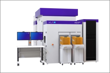
KLA Announces eSL10 Electron-Beam Patterned Wafer Defect Inspection System
KLA announced eSL10, an electron beam pattern wafer defect inspection system. The eSL10 is designed to detect and report defects that cannot be detected by conventional optical equipment or other electron beam defect inspection platforms, thereby accelerating the time-to-market for high-performance logic and memory semiconductor chips, including semiconductor chips manufactured through EUV lithography processes.
2020.07.22by 이수민 기자

Samsung Electronics Ships First EUV Process-Applied DRAM at Pyeongtaek Line 2
Samsung Electronics announced the commencement of operations at Pyeongtaek Line 2, the world's largest semiconductor production line. The line will produce third-generation 10-nanometer-class LPDDR5 mobile DRAM with EUV process technology applied for the first time in the industry. Additionally, the company plans to manufacture next-generation V-NAND and ultra-fine-pitch foundry products starting from the second half of 2021.
2020.08.31by 이수민 기자

Intel Unveils Next-Generation 'Core Ultra Series 3' and vPro Platform for Enterprise PCs
Intel has officially unveiled the "Intel Core Ultra Series 3" for next-generation enterprise PCs and the latest vPro platform, addressing a wide range of demands from enterprise notebooks to high-performance workstations.
2026.03.26by 배종인 기자

ROHM Launches ESD Protection Diode Compatible with High-Speed Interfaces of 10Gbps or Higher
Semiconductor specialist ROHM has developed the 'RESDxVx series' of ESD (electrostatic discharge) protection diodes capable of responding to next-generation high-speed data communication environments exceeding 10Gbps, simultaneously enhancing both signal quality maintenance required in high-speed interfaces and IC protection performance.
2026.03.26by 배종인 기자











