


KERI develops technology and equipment for early analysis of SiC material crystal defects.
 Published2021.03.10 10:10
Early observation of invisible SiC crystal defects
Developing equipment with Etamax, half the price of Japanese equipment
Silicon carbide (SiC) has recently been gaining attention as a power semiconductor material due to its superior durability, versatility, and efficiency compared to silicon (Si). However, SiC has invisible internal crystal defects (dislocations) that can reduce the performance of semiconductor devices.
The Korea Electrotechnology Research Institute (KERI) Power Semiconductor Research Center's Dr. Bang Wook and Dr. Na Moon-kyung's team announced on the 8th that they have developed a technology to analyze and evaluate crystal defects in SiC materials at an early stage.
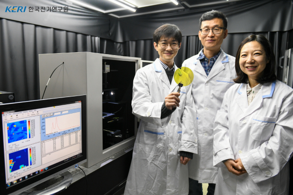
Researchers Jeong Hyeon-jin, Bang Wook, and Na Moon-kyung [Photo = KERI]
Crystal defects are complex and difficult to identify. They can degrade the characteristics of semiconductor devices from the very beginning of their operation, and in some cases, their characteristics can change during use, causing problems. If a problem occurs in SiC power semiconductors in power grid equipment or electric vehicles on the road, it could result in serious damage to life and property. This is why analytical technology is crucial.
Defects in SiC materials are invisible, and the material itself is hard, making observation difficult. Currently, the technology for SiC material inspection equipment is so complex and the barriers to entry are high, with Japan holding over 80% of the global market. Due to the high equipment prices, performance testing in Korea is limited to a limited number of wafer samples. Accordingly, the research team developed a technology for detecting defects in SiC materials using the photoluminescence (PL) phenomenon for the first time in Korea.
PL analysis analyzes the phenomenon in which excited electrons emit light of a specific wavelength as they return to their original positions. This involves sending ultraviolet (UV) energy to SiC material and analyzing the specific wavelengths emitted by the electrons to determine whether they are normal or not.
SiC is an indirect semiconductor material with low PL emission efficiency, making signal detection difficult. The research team, in collaboration with Etamax Co., Ltd., a company specializing in optical inspection equipment, developed a "SiC material defect analysis device for power semiconductors" that reduces PL loss.
Unlike Japanese products that detect surface and internal defects by selecting two different wavelengths of light depending on the inspection target and evaluation items, the newly developed equipment uses a single laser wavelength to detect various internal defects without destroying the SiC material. The research team stated, "The equipment's performance is equal to or better than that of the Japanese equipment," and added, "We expect to be able to supply it at half the price of the Japanese product, which costs approximately 1.4 billion won."
Dr. Moon-Kyung Na of KERI stated, "Through continued research, we will expand the evaluation scope to include broadband semiconductor materials such as diamond, and strive to diversify and refine our analysis techniques." The research team has completed a patent application for the technology and plans to continue working with Etamax to upgrade the equipment and accelerate commercialization.
Meanwhile, market research firm IHS Markit forecasted that the SiC power semiconductor market size would grow by an average of 32% annually from approximately $700 million (approximately KRW 780 billion) in 2020 to approximately $10 billion (approximately KRW 11.14 trillion) in 2030.
Comments
Related news
KERI Develops Elastic Wave Sensor with Built-in Preamplifier for Fault Prediction
Dr. Kim In-sung's team at the Electrical Materials Conversion Research Center of the Korea Electrotechnology Research Institute has developed an electrical sensor technology with a built-in preamplifier that can detect elastic waves—minute vibrations transmitted from elastic materials—to pre-diagnose signs of deterioration or malfunction in various equipment and facilities. This technology is expected to be primarily applied in safety diagnosis fields within the energy industry.
2020.11.13by 이수민 기자
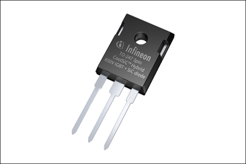
Infineon Launches 'Si+SiC' 650V Hybrid IGBT Family
Infineon launches a 650V CoolSiC hybrid IGBT discrete product family. The product family combines 650V TRENCHSTOP 5 IGBT technology with a unipolar Schottky barrier CoolSiC diode. With high switching frequency and low switching loss, it is suitable for DC/DC converters and PFC, and can be utilized in battery charging infrastructure, energy storage solutions, solar inverters, UPS, server and telecom SMPS applications.
2021.02.18by 강정규 기자
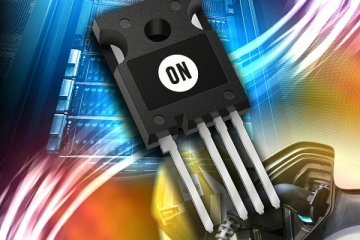
ON Semiconductor Unveils AEC-Q101 Compliant 650V SiC MOSFETs
ON Semiconductor has unveiled a new product family of 650V silicon carbide MOSFETs. The new products, which replace conventional silicon devices, are suitable for applications including electric vehicle on-board chargers, server power supplies, uninterruptible power supplies, solar inverters, and telecommunications.
2021.02.19by 강정규 기자

Intel Unveils Next-Generation 'Core Ultra Series 3' and vPro Platform for Enterprise PCs
Intel has officially unveiled the "Intel Core Ultra Series 3" for next-generation enterprise PCs and the latest vPro platform, addressing a wide range of demands from enterprise notebooks to high-performance workstations.
2026.03.26by 배종인 기자

ROHM Launches ESD Protection Diode Compatible with High-Speed Interfaces of 10Gbps or Higher
Semiconductor specialist ROHM has developed the 'RESDxVx series' of ESD (electrostatic discharge) protection diodes capable of responding to next-generation high-speed data communication environments exceeding 10Gbps, simultaneously enhancing both signal quality maintenance required in high-speed interfaces and IC protection performance.
2026.03.26by 배종인 기자











