


"SiC and GaN-based semiconductor market shows clear growth trend"
 Published2021.03.13 15:45
Following 5G and EVs, demand in the cloud and AI sectors is on the rise.
ON Semi Completes SiC Process Development... Developing SiC Substrates
The utilization of wide-bandgap (WBG) semiconductors based on silicon carbide (SiC) and gallium nitride (GaN) materials, which allow for higher voltages and lower losses than conventional silicon (Si)-based semiconductors, is increasing.
ON Semiconductor recently expanded its WBG device family with the launch of 650V SiC MOSFETs, providing improved efficiency in previously underserved power bands. The following is a Q&A with Brandon Becker, Product Line Manager at ON Semiconductor, regarding the 2021 market outlook.
Q. The adoption of WBG semiconductors based on SiC and GaN is notable in emerging fields such as 5G and electric vehicles (EVs). However, conventional Si-based semiconductors still hold a significant market share. How do you forecast the SiC and GaN-based semiconductor sectors for this year?
A. Semiconductors utilizing SiC and GaN materials will continue to be applied in applications requiring high efficiency and power density. In terms of cost, adopting WBG semiconductors can reduce overall system costs. For example, designers can eliminate application cooling systems and reduce the size and cost of passive components. This is possible because WBG semiconductors have higher switching frequencies than Si-based semiconductors. Solutions combining the two semiconductors will soon emerge. For example, there are inverters that combine Si IGBTs and SiC diodes to reduce system costs while increasing efficiency and reliability.
Q. How much are the application cases of SiC MOSFETs increasing in the 5G field?
A. 5G theoretically offers communication speeds 20 times faster than LTE. However, implementing high-speed communication requires devices that can handle more power, possess excellent thermal efficiency to prevent hardware overheating, and are optimized for power efficiency. SiC materials are highly suitable for use in demanding environments, enabling SiC MOSFETs to achieve these performance goals. Furthermore, leveraging these advantages, SiC will play a critical role in the provision of cloud and AI services. Currently, demand for applications in this field is increasing significantly, and the requirement for high power density is a major concern for designers.

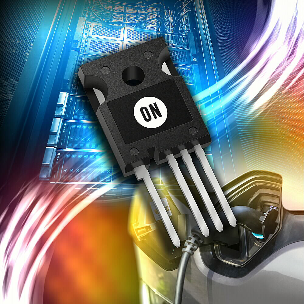
[Graphic by ON Semiconductor]
Q. What are the unique differentiating features of ON Semi's SiC MOSFETs compared to devices from other companies?
A. ON Semi possesses various competitive advantages, including an internal supply chain, manufacturing expertise, proven SiC MOSFET device performance offered at reasonable prices, and highly regarded customer support. ON Semi holds the second-largest position in the global power semiconductor industry and maintains close relationships with customers, playing a critical role in their system designs. To date, ON Semi has expanded its 900V and 0200V SiC MOSFET product families. This year, we announced 650V SiC MOSFET technology and are working with customers in the early engineering stages to implement it.
Once this technology is officially launched, we plan to focus on maximizing production capacity to provide the short lead times required by our customers. Additionally, we are continuously collaborating with customers across a diverse range of applications, including automotive traction inverters, onboard chargers, EV charging systems, solar generators, solar inverters, server power supplies, and telecommunications and uninterruptible power supplies. Furthermore, we are meeting the demand for WBG technology in fields such as professional lighting and audio, medical, power tools, appliances, and auxiliary motors.
Q. Are there any instances where ON Semi's SiC devices have been applied to EVs?
A. ON Semi is working closely with automotive companies around the world. Currently, SiC MOSTFETs and diodes are being applied to various EVs. In particular, we are conducting various collaborative projects with OEMs in the global automotive industry, and the progress varies depending on the product, qualification, evaluation, and development type. ON Semi also provides various EV reference designs to customers.

ON Semi, which provides the design [Photo = ON Semiconductor]
Q. What is the basis for the competitiveness of the new 650V SiC MOSFET?
A. ON Semi SiC MOSFETs are fabricated according to a new active cell design utilizing advanced thin wafer technology capable of achieving industry-leading Rsp(RDS(on)×area) at a breakdown voltage of 650V. Available in D2PAK7L and To247 packages, the NVBG015N065SC1, NTBG015N065SC1, NVH4L015N065SC1, and NTH4L015N065SC1 SiC MOSFETs provide an on-resistance of 12mΩ (milliohm).
ON Semi's latest wafer technology is optimized for energy loss figures, providing optimal performance for automotive and industrial applications. The use of internal gate resistance (Rg) offers greater design flexibility, as designers no longer need to artificially reduce device speeds by adding external gate resistance. In addition, it withstands high surges and avalanches, provides short-circuit robustness to enhance durability and reliability, and extends device lifespan.
Q. How do you foresee the future direction of Si, SiC, and GaN materials?
A. SiC and GaN materials will become essential components of future electronic devices. Even now, based on their unique physical properties, these two materials are enabling the creation of devices that were previously impossible to manufacture. SiC MOSFETs have been perfected over the past 50 years and continue to be steadily improved. ON Semi is customizing WBG technology for specific applications. Furthermore, we aim to help customers achieve their goals by continuously innovating advanced devices that push beyond what they consider possible limits.
Q. What are the fields where SiC and GaN semiconductors will be most widely used within the next 2 to 3 years?
A. We expect the market share of SiC in industrial power and energy generation applications to steadily expand. In particular, we anticipate rapid growth in the automotive traction inverter sector. GaN materials are expected to be widely adopted in applications such as consumer power supplies, where power density is a design priority. While they can be applied to other more demanding applications, adoption rates will not reach the same level as the consumer sector for the next approximately three years.
Q. How did ON Semi overcome the difficulties in developing SiC MOSFETs?
A. The biggest challenge currently is the development of SiC substrates, and semiconductor manufacturers, including ON Semiconductor, are making significant efforts to address this. SiC substrates are very different from conventional Si boules. Everything related to production, from the equipment used to the processes, handling methods, and cutting methods, must be specially developed for SiC materials.
ON Semi has conducted extensive R&D to reduce defect density, thereby improving its cost structure. As a result, the adoption of SiC MOSFETs among customers is accelerating. Other challenges include epitaxial growth, fab processing, and packaging, but they are not limited to these areas. Each individual supply chain stage presents unique engineering challenges that must be addressed on a daily basis.
Q. It seems the COVID-19 pandemic has affected the supply of SiC raw materials as well as the design, manufacturing, and supply of SiC MOSFETs. What are ON Semi's countermeasures?
A. ONSemi closely monitors all raw material supplies. By maintaining multiple verified suppliers, we ensure supply continuity and enable rapid response. In addition, we operate expert teams at various internal and external locations to certify our products and are taking every precaution to ensure that SiC device manufacturing is never interrupted at any branch.
Comments
Related news
Infineon Launches 'Si+SiC' 650V Hybrid IGBT Family
Infineon launches a 650V CoolSiC hybrid IGBT discrete product family. The product family combines 650V TRENCHSTOP 5 IGBT technology with a unipolar Schottky barrier CoolSiC diode. With high switching frequency and low switching loss, it is suitable for DC/DC converters and PFC, and can be utilized in battery charging infrastructure, energy storage solutions, solar inverters, UPS, server and telecom SMPS applications.
2021.02.18by 강정규 기자
ON Semiconductor Unveils AEC-Q101 Compliant 650V SiC MOSFETs
ON Semiconductor has unveiled a new product family of 650V silicon carbide MOSFETs. The new products, which replace conventional silicon devices, are suitable for applications including electric vehicle on-board chargers, server power supplies, uninterruptible power supplies, solar inverters, and telecommunications.
2021.02.19by 강정규 기자
KERI develops technology and equipment for early analysis of SiC material crystal defects.
Silicon carbide (SiC) is gaining attention as a power semiconductor material that offers superior durability, versatility, and efficiency compared to silicon (Si). However, SiC material contains invisible internal crystal defects that can degrade the performance of semiconductor devices. In response, a research team led by Dr. Bang Wook and Dr. Na Moon-kyung at the Power Semiconductor Research Center of the Korea Electrotechnology Research Institute (KERI) has developed a technology to analyze and evaluate crystal defects in SiC material at an early stage.
2021.03.10by 이수민 기자

Intel Unveils Next-Generation 'Core Ultra Series 3' and vPro Platform for Enterprise PCs
Intel has officially unveiled the "Intel Core Ultra Series 3" for next-generation enterprise PCs and the latest vPro platform, addressing a wide range of demands from enterprise notebooks to high-performance workstations.
2026.03.26by 배종인 기자

ROHM Launches ESD Protection Diode Compatible with High-Speed Interfaces of 10Gbps or Higher
Semiconductor specialist ROHM has developed the 'RESDxVx series' of ESD (electrostatic discharge) protection diodes capable of responding to next-generation high-speed data communication environments exceeding 10Gbps, simultaneously enhancing both signal quality maintenance required in high-speed interfaces and IC protection performance.
2026.03.26by 배종인 기자











