


Key Foundry Begins Full-Scale Mass Production of Automotive Semiconductors
 Published2021.04.08 11:12
Application in various products such as touch ICs and wireless charging ICs is expected.
 Amid the recent worsening shortage of automotive semiconductors, Key Foundry (CEO Lee Tae-jong), Korea's only pure foundry semiconductor company, is set to begin full-scale mass production of automotive semiconductors.
Key Foundry announced on the 6th that it has recently completed the development of its first automotive semiconductor using the second-generation 0.13 micron Embedded Flash process and will begin full-scale mass production within the year.
Key Foundry has been mass-producing the first-generation 0.13 micron Embedded Flash Technology developed for consumers for over five years, and this process is being used in various products such as MCUs, Touch, and Auto Focus.
The newly developed 2nd generation 0.13 micron Embedded Flash Technology was developed to meet AEC-Q100 Grade-1 reliability standards so that it can be used in automotive semiconductor products.
AEC-Q100 Grade-1, a reliability test standard for automotive electronic components, is a very stringent reliability standard that requires all functions of a semiconductor chip to operate normally for more than 10 years at a high temperature of 125°C and all information stored in Flash to be retained for more than 10 years.
Key Foundry, based on the robust characteristics of its proprietary Side-wall Selective Transistor Cell (SSTC) structure and accumulated know-how, AEC-Q100 Grade-1 reliability testWe passed all tests and developed Embedded Flash Technology suitable for the development of automotive semiconductor products by significantly improving the reliability of Flash Memory through the design of adding ECC (Error Correcting Code Memory) within the Embedded Flash IP.
Key Foundry announced that its second-generation 0.13 micron Embedded Flash process has been applied for the first time to an automotive Hi-Pass terminal MCU product for a domestic customer. The product utilizes the 128Kbyte eFlash IP and process provided by Key Foundry, and after completing all product-level verification, it will begin full-scale mass production starting this year.
This is the first automotive semiconductor product utilizing Key Foundry's Embedded Flash process, and with the successful development of this product, we expect its application to expand to various products in the future, such as automotive touch ICs and automotive wireless charging ICs.
The second-generation 0.13 micron Embedded Flash Technology offers improved reliability compared to the existing first-generation process while maintaining competitiveness in terms of process costs, making it applicable not only to automotive products but also to consumer products such as MCUs, Touch, and Auto Focus.
In addition, by integrating with the BCD (Bipolar-CMOS-DMOS) process, it is possible to expand into various power semiconductor products such as USB Type-C PD, motor driver ICs, and wireless charging ICs, and it is expected to be utilized in low-power IoT products through the Ultra Low Leakage process option.
Key Foundry is developing 0.11 micron Embedded Flash Technology following the 1st and 2nd generation 0.13 micron Embedded Flash. With the recent increase in customer demand for high memory density, we plan to provide Flash IP with up to 4Mbits memory density by drastically reducing the number of Flash Cells in the future.
"With the automotive semiconductor market growing rapidly recently, I am pleased that the first automotive semiconductor product utilizing Key Foundry's second-generation 0.13 micron Embedded Flash Technology has completed development and entered mass production," said Lee Tae-jong, CEO of Key Foundry. "Based on the technology we have accumulated, Key Foundry will provide foundry technology with a very high level of reliability and cost competitiveness, and we plan to continuously increase the proportion of automotive semiconductor products based on this technological capability."

Comments
Related news

MagnaChip Sells Foundry Business to Private Equity Fund Involved SK Hynix
Magnachip has concluded a contract to sell its foundry business division and Cheongju plant to an SPC funded by Saemaul Geumgo Central Association and SK Hynix. Through this sale, Magnachip has decided to focus on its display solution business and power solution business.
2020.04.01by 이수민 기자
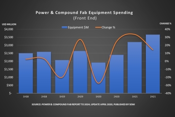
Power semiconductor fab equipment investment is expected to reach a record high in 2021.
SEMI forecasts that power and compound semiconductor fab equipment investment will rebound in the second half of this year, and is projected to reach a record high of $6.9 billion next year, representing 59% growth compared to this year. As of 2019, 804 power and compound semiconductor production facilities were equipped with monthly wafer production capacity of approximately 8 million wafers based on 200mm wafers, and by 2024, 38 new production facilities are expected to begin operations, with production volume projected to increase by approximately 20% to 9.6 million wafers per month.
2020.05.06by 이수민 기자
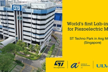
ST establishes world's first LiF plant to expand piezoelectric MEMS market
ST Microelectronics (hereinafter ST), in collaboration with the Institute of Microelectronics under A*STAR (Agency for Science, Technology and Research, Singapore, hereinafter A*STAR) and Axcelis, a leading manufacturing tool supplier from Japan, will jointly establish and operate an 8-inch (200mm) R&D line focused on piezo MEMS technology. This collaboration will strengthen ST Singapore's manufacturing process portfolio and accelerate the adoption of piezo MEMS actuators in emerging application fields. These include MEMS mirrors for smart glasses and AR headsets, LiDAR systems, PMUTs (Piezoelectric Micromachined Ultrasonic Transducers) for new medical applications, and piezo heads supporting commercial and industrial 3D printing.
2020.11.03by 김동우 기자

Intel Unveils Next-Generation 'Core Ultra Series 3' and vPro Platform for Enterprise PCs
Intel has officially unveiled the "Intel Core Ultra Series 3" for next-generation enterprise PCs and the latest vPro platform, addressing a wide range of demands from enterprise notebooks to high-performance workstations.
2026.03.26by 배종인 기자

ROHM Launches ESD Protection Diode Compatible with High-Speed Interfaces of 10Gbps or Higher
Semiconductor specialist ROHM has developed the 'RESDxVx series' of ESD (electrostatic discharge) protection diodes capable of responding to next-generation high-speed data communication environments exceeding 10Gbps, simultaneously enhancing both signal quality maintenance required in high-speed interfaces and IC protection performance.
2026.03.26by 배종인 기자











