


KAIST Boosts Communication Chip Performance with Semiconductor 3D Stacking Technology
 Published2021.06.15 10:10
III-V HEMT integration on Si CMOS substrate
100nm process approaches 10nm performance
Communication and quantum signals are analog, which means they can become weaker or more susceptible to noise during transmission, leading to signal distortion. Therefore, high-speed signal amplification is essential for transmitting and receiving signals. These amplification devices require characteristics such as ultra-high speed, high output, low power, and low noise. Furthermore, with the advancement of communication technologies like 5G, the systems that comprise them are becoming increasingly complex, further increasing the importance of highly integrated component manufacturing technology.

Jaeyong Jeong, PhD candidate [Photo = KAIST]
The Korea Advanced Institute of Science and Technology (KAIST) announced on the 14th that a research team led by Professor Sang-Hyun Kim of the Department of Electrical and Electronic Engineering has developed a compound semiconductor device technology based on monolithic 3D integration that overcomes the shortcomings of existing communication devices. Monolithic 3D integration is a technology that forms an upper thin film layer after the lower device process and then performs the upper device process to improve the alignment of the upper and lower devices.
There are two common ways to implement communication components.
This is a method of implementing an amplifier element using high-density Si CMOS using silicon (Si), and a method of manufacturing an amplifier element using III-V compound semiconductors and packaging other elements using Si CMOS. III-V compound semiconductors are semiconductors formed by compounds of group III elements and group V elements, and have excellent charge transport properties and optical properties.
However, Si technology faces limitations in its physical properties, making it difficult to improve critical device performance, such as cutoff frequency characteristics, for communication devices. There's also the problem of increased noise due to signal interference, such as substrate coupling noise. III-V technology offers superior device noise characteristics, but its integration and packaging processes with other components are complex. The packaging process can also lead to signal loss issues.
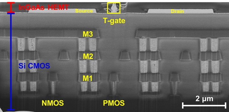
A KAIST research team has developed a process and device structure that maximizes the advantages of both devices by three-dimensionally integrating III-V HEMTs (High-Electron Mobility Transistors), which boast superior analog signal amplification performance, onto a Si CMOS substrate. This method involves stacking the devices in three layers and integrating them on the same substrate. At the same time, the team demonstrated the ability to eliminate noise caused by substrate signal interference.
The research team utilized ultra-low-temperature processes, such as wafer bonding, to integrate the upper III-V devices at temperatures below 300°C, maintaining the performance of the underlying Si CMOS even after the upper device integration. Furthermore, by introducing an InGaAs/InAs/InGaAs quantum well structure to fabricate the upper III-V devices, they realized electron transport characteristics. It was also revealed that superior performance can be achieved without using a sub-10nm process by using a 100nm (nanometer) process.
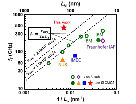
[Image = KAIST]
In addition, it was experimentally demonstrated for the first time that the noise caused by substrate interference in existing SI CMOS can be resolved by fabricating the device in a three-dimensional integrated form.
Professor Kim Sang-hyun said, “This technology can also be applied to quantum qubit decryption circuits,” and added, “We will focus on follow-up research to ensure that it can be utilized in various fields.”
Meanwhile, this study was conducted by KAIST Department of Electrical and Electronic Engineering Ph.D. candidate Jaeyong Jeong, with the first author, in collaboration with a research team led by Dr. Jongmin Kim of the Korea Institute of Nanotechnology and Professor Jaehyung Jang of the Gwangju Institute of Science and Technology. The research was also presented at the 'Symposium on VLSI Technology.'
Comments
Related news
LG Electronics, Keysight, and KAIST to Collaborate on 6G Mobile Communication Technology Development
6G technology is considered a means to enable Ambient Internet of Everything (AIoE) with maximum data transmission of 1Tbps per second. LG Electronics, Keysight Technologies, and Korea Advanced Institute of Science and Technology (KAIST) have signed an MOU for technology development and verification system establishment to secure market dominance in 6G technology, with standardization expected in 2025 and commercialization anticipated in 2029.
2021.03.23by 이수민 기자
"High-density, compact PCB implementation depends on resistor utilization"
Components on PCBs have different operating voltages. If the input voltage is lower than the operating voltage, the component will not function. Conversely, if the input voltage is higher, excessive current flows and causes failure. In this case, a resistor is needed to control the flow of current and enable the component to operate smoothly.
2021.05.31by 이수민 기자
.jpg)
Samsung Electronics Develops 8-Nan RF Process Technology
Samsung Electronics is aggressively pursuing the 5G communication semiconductor market from sub-6GHz to millimeter wave (mmWave) by providing RF chips for 5G communication supporting multi-channel and multi-antenna as a single-chip solution through its 8-nano RF foundry process.
2021.06.09by 배종인 기자

Intel Unveils Next-Generation 'Core Ultra Series 3' and vPro Platform for Enterprise PCs
Intel has officially unveiled the "Intel Core Ultra Series 3" for next-generation enterprise PCs and the latest vPro platform, addressing a wide range of demands from enterprise notebooks to high-performance workstations.
2026.03.26by 배종인 기자

ROHM Launches ESD Protection Diode Compatible with High-Speed Interfaces of 10Gbps or Higher
Semiconductor specialist ROHM has developed the 'RESDxVx series' of ESD (electrostatic discharge) protection diodes capable of responding to next-generation high-speed data communication environments exceeding 10Gbps, simultaneously enhancing both signal quality maintenance required in high-speed interfaces and IC protection performance.
2026.03.26by 배종인 기자











