


Applied Materials Accelerates Heterogeneous Convergence in the Semiconductor Industry
 Published2021.09.16 09:27
▲Applied Materials heterogeneous combination design image
Applied Materials, a global leader in materials engineering solutions, announced new technologies and capabilities for heterogeneous chip design and integration.
Applied Materials announced on the 16th that it is collaborating with leaders in advanced packaging and large-area substrates to simultaneously improve solution delivery speed and PPACt (power, performance, size, cost, and time to market).
Applied Materials' announcements of die-to-wafer hybrid bonding, wafer-to-wafer bonding, and advanced substrate technologies revolutionize advanced packaging for heterogeneous integration. Heterogeneous integration allows semiconductors of various technologies, functions, and sizes to be manufactured in a single package, offering semiconductor and systems companies new types of design and production flexibility.
Applied Materials is the leading supplier of advanced packaging, offering optimal products covering etching, PVD (physical vapor deposition), CVD (chemical vapor deposition), electroplating, surface treatment, and annealing. Applied's Advanced Packaging Development Center in Singapore has the broadest portfolio of technologies that form the foundation for heterogeneous integration, including advanced bumps, microbumps, fine-line redistribution layers (RDLs), through-silicon vias (TSVs), and hybrid bonding.
“Applied Materials’ industry-leading advanced packaging portfolio provides customers with a broad range of options for implementing heterogeneous integration technologies,” said Nirmalya Maity, vice president of Advanced Packaging at Applied Materials. “Through technology co-optimization and collaboration with other companies, we are accelerating our customers’ PPACt roadmaps and fostering an ecosystem that creates new growth opportunities.”
Die-to-wafer hybrid bonding increases I/O density through direct copper-to-copper interconnection, reducing interconnect length between chiplets and improving overall performance, power, and cost. To accelerate technology development, Applied Materials has introduced advanced software modeling and simulation to its Advanced Packaging Development Center in Singapore.
These capabilities enable Applied to evaluate and optimize factors such as material selection and packaging architecture before hardware development, shortening learning cycles and time-to-market. This builds on a joint development agreement announced last October between Applied Materials and BE Semiconductor Industries (Besi) to develop the industry's first complete and proven equipment for die-based hybrid bonding.
“Our joint development program with Applied Materials has significantly enhanced Besi’s understanding of the co-optimized solutions our customers need to leverage complex hybrid bonding processes in wafer-level production environments,” said Ruurd Boomsma, Besi’s Chief Technology Officer. “Besi and Applied have achieved exceptional results in a very short period of time in our hybrid bonding Center of Excellence in Singapore, enabling our customers to process their materials and develop advanced heterogeneous bonding technologies.”
Wafer-to-wafer bonding technology allows semiconductor structures to be implemented on a first wafer, other components on a second wafer, and then the two wafers are bonded together to create a complete device. To achieve high performance and yield, the quality of the preprocessing steps, including precise uniformity and alignment during the wafer bonding process, is crucial.
Applied Materials has signed a joint development agreement with EV Group (EVG) to develop a joint optimization solution for wafer-to-wafer bonding. This collaboration is expected to leverage synergy between Applied Materials' semiconductor process expertise in deposition, planarization, implantation, metrology, and inspection, and EVG's leadership in wafer bonding, preprocessing, activation, alignment, and bond overlay metrology.

Comments
Related news

Applied Materials Accelerates Semiconductor Innovation with its AIx Platform
Applied Materials, a global leader in materials engineering solutions, is actively accelerating semiconductor technology innovation that bridges the lab to fab by leveraging big data and AI capabilities.
2021.04.27by 배종인 기자

Applied Materials, 3Q Revenue $6.196 Billion…Up 41% Year-over-Year
Applied Materials, the global leader in materials engineering solutions, achieved record-breaking results in the third quarter of fiscal year 2021 with revenue of $6.196 billion, driven by surging semiconductor demand.
2021.08.23by 배종인 기자
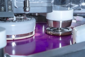
Applied Materials Unveils Two Types of SiC Wafer Equipment
SiC material is sensitive to native defects compared to Si, which can degrade electrical performance, power efficiency, reliability, and yield. Therefore, optimizing wafer mass production and minimizing crystal lattice damage are challenging. In response, Applied Materials has unveiled two types of equipment to support SiC semiconductor manufacturers in transitioning from 150mm to 200mm wafer production systems.
2021.09.14by 이수민 기자

Intel Unveils Next-Generation 'Core Ultra Series 3' and vPro Platform for Enterprise PCs
Intel has officially unveiled the "Intel Core Ultra Series 3" for next-generation enterprise PCs and the latest vPro platform, addressing a wide range of demands from enterprise notebooks to high-performance workstations.
2026.03.26by 배종인 기자

ROHM Launches ESD Protection Diode Compatible with High-Speed Interfaces of 10Gbps or Higher
Semiconductor specialist ROHM has developed the 'RESDxVx series' of ESD (electrostatic discharge) protection diodes capable of responding to next-generation high-speed data communication environments exceeding 10Gbps, simultaneously enhancing both signal quality maintenance required in high-speed interfaces and IC protection performance.
2026.03.26by 배종인 기자











