



SK Hynix Develops HBM3, the Fastest DRAM to Date
 Published2021.10.20 09:22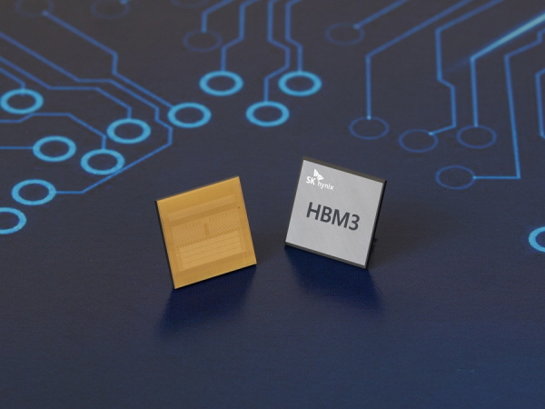
Utilizing high-performance data centers, machine learning, and supercomputers
SK Hynix has developed the highest-spec DRAM available, capable of processing data equivalent to 163 ultra-high-definition movies in just one second. This is expected to be used in high-performance data centers, machine learning, and supercomputers.
SK Hynix announced on the 20th that it has developed the industry's first 'HBM3' DRAM.
HBM (High Bandwidth Memory) is a high-value, high-performance product that vertically connects multiple DRAMs to dramatically increase data processing speeds compared to conventional DRAM. HBM3 is the fourth-generation HBM product.
SK Hynix solidified its leadership in this market by developing HBM3 just one year and three months after becoming the first in the industry to begin mass production of HBM2E DRAM in July of last year.
SK Hynix emphasized, “With this HBM3, we have not only achieved the highest speed and largest capacity among HBM DRAMs released so far, but also significantly improved the quality level.”
In terms of speed, HBM3 can process 819GB (gigabytes) of data per second. This is equivalent to processing 163 5GB full-HD movies in just one second. Compared to the previous generation HBM2E, the speed is about 78% faster.
Additionally, this product incorporates on-die error correction code (ECC). This code allows HBM3 to automatically correct errors in data transmitted to DRAM cells, significantly enhancing product reliability.
This HBM3 will be released in two capacities: 16GB and 24GB. The 24GB option, in particular, represents the industry's largest. To achieve this, SK Hynix engineers ground individual DRAM chips to a height of approximately 30 micrometers (μm, 10-6m), roughly one-third the thickness of a sheet of A4 paper, and then vertically connected twelve of these chips using TSV technology.
TSV (Through Silicon Via) is an interconnection technology that drills thousands of tiny holes in a DRAM chip and connects the upper and lower layer chips with electrodes that vertically penetrate the holes.
In the future, HBM3 will be installed in high-performance data centers and is expected to be applied to supercomputers used in machine learning, which enhances the perfection of artificial intelligence (AI), climate change analysis, and new drug development.
SK Hynix Vice President Cha Seon-yong (in charge of DRAM development) said, “As the world’s first company to launch HBM DRAM, we led the HBM2E market and succeeded in developing HBM3 for the first time in the industry.” He added, “We will continue to solidify our leadership in the premium memory market while doing our best to increase customer value by supplying products that comply with ESG management.”

Comments
Related news
SK Hynix Mass-produces 128-Layer 4D SSD for Data Centers
SK Hynix has commenced mass production of a new enterprise SSD product that secures competitive advantage in high performance and low power consumption. The enterprise SSD product lineup now encompasses both SATA and PCIe form factors. Internal certification of the product was completed at the end of March, and it is scheduled to be provided to major customers during May.
2021.04.15by 배종인 기자
SK Hynix mass-produces 10nm-class '1a' DRAM based on EUV process
SK Hynix announced that it has begun mass production of 8Gbit LPDDR4 mobile DRAM applying 10-nanometer class 1a process technology. 1a is a technology following 1x, 1y, 1z, and products will be supplied from the second half of the year. Additionally, it marks the first DRAM product from SK Hynix to be mass-produced using EUV process.
2021.07.13by 이수민 기자
SK Hynix Launches 2TB SSD for Consumers
SK Hynix has simultaneously launched a 2TB (terabyte) capacity product in its consumer SSD 'Gold P31' lineup in both Korea and the United States.
2021.08.19by 배종인 기자

Intel Unveils Next-Generation 'Core Ultra Series 3' and vPro Platform for Enterprise PCs
Intel has officially unveiled the "Intel Core Ultra Series 3" for next-generation enterprise PCs and the latest vPro platform, addressing a wide range of demands from enterprise notebooks to high-performance workstations.
2026.03.26by 배종인 기자

ROHM Launches ESD Protection Diode Compatible with High-Speed Interfaces of 10Gbps or Higher
Semiconductor specialist ROHM has developed the 'RESDxVx series' of ESD (electrostatic discharge) protection diodes capable of responding to next-generation high-speed data communication environments exceeding 10Gbps, simultaneously enhancing both signal quality maintenance required in high-speed interfaces and IC protection performance.
2026.03.26by 배종인 기자











