


Solving the Limitations of Semiconductor Vertical Stacking and FinFET
 Published2021.12.17 14:25
Easing physical constraints and solving scaling challenges
Samsung's 5nm Manufacturing Continues IBM-Samsung Design Collaboration
Vertical device architecture technology is emerging to overcome the physical limitations of FinFET-based process technology that stacks transistors along the wafer plane, raising expectations that it will solve existing scaling challenges and meet the demand for high-performance computing semiconductors.
IBM and Samsung Electronics announced on the 15th a new semiconductor design, the Vertical-Transport Nanosheet Field Effect Transistor (VTFET), that utilizes a vertical transistor architecture.
This semiconductor processing technology stacks transistors vertically on the chip surface, rather than flat, allowing current to flow vertically or vertically. This is said to alleviate physical constraints on transistor length, spacer thickness, and contact size, thereby resolving scaling challenges.
The existing flagship technology, FinFET, is currently evaluated to have reached its limits as it stacks transistors along the wafer plane, leaving very little space for spacers, gates, and contacts.
The VTFET process allows chip designers to pack more transistors into a given area, overcoming the limitations of Moore's Law and addressing many of the barriers to increased performance. Additionally, it improves transistor contact points, reducing power waste while allowing more current to flow. Overall, the new process technology can deliver twice the performance or 85% power savings compared to existing finFET process chips.
Additionally, the newly developed chip is expected to be produced on Samsung Electronics' 5nm node.
The chips produced this way are expected to be utilized in IBM's own server platforms. Following Samsung's announcement in 2018 that it would manufacture IBM's 7nm chips, these chips were incorporated into IBM's Power10 server lineup earlier this year. Additionally, the IBM Telum Processor, which was unveiled earlier this year, is also a product manufactured by Samsung based on IBM's design.
This announcement is particularly noteworthy because it comes amid a global semiconductor shortage that has highlighted the importance of investment in chip research and development, as well as the growing importance of semiconductors themselves for use in computers, consumer electronics, communications equipment, transportation systems, and critical infrastructure.
As new VTFET architectures are developed, the semiconductor industry will be able to continue to push the boundaries of nanofabrication to expand semiconductor performance and continue to innovate, such as enabling cell phone batteries that can last for a week, not just days, without a charge.
In addition, it is expected that △ power usage and carbon emissions will be reduced for tasks that require high power, such as cryptocurrency mining and data encryption, and △ support will be provided for the continued expansion of low-power consumption Internet of Things (IoT) and edge devices so that these devices can be operated in a wider range of environments, such as marine buoys, autonomous vehicles, and spacecraft.
“The technologies we’re announcing today challenge conventions, deliver new innovations that improve our lives and businesses, reduce our environmental impact, and rethink how we move the world forward,” said Mukesh Khare, vice president of Hybrid Cloud and Systems at IBM Research. “Even as the semiconductor industry faces challenges across multiple sectors, IBM and Samsung are demonstrating their commitment to pursuing ‘hard tech,’ not just innovation in semiconductor design.”
Meanwhile, NH Investment & Securities researcher Do Hyeon-woo said that if connected to mass production, it will lead to a significant improvement in semiconductor device performance, contributing to the increase in demand for high-performance operations, and considering the device characteristics, in the equipment field, CVD Selective MetIt is expected that AMAT, which is developing Al Capping equipment, and Lam Research, which is developing Atomic Layer Etch equipment, will benefit.

Comments
Related news
IBM Unveils 2nm Chip, Expected to Applied to IBM Power Systems by the End of the Year
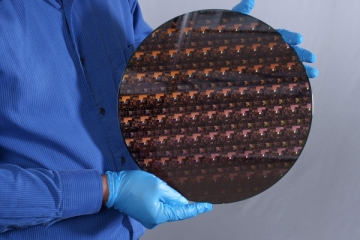
IBM has unveiled a chip developed with 2nm nanosheet technology. The new 2-nanometer chip features up to 50 billion transistors, delivering 45% higher performance than today's most advanced 7-nanometer node chips while consuming 75% less energy. IBM's first commercialized 2-nanometer chip, which includes an upgraded version of the 7-nanometer chip from IBM's Albany Research Laboratory, is expected to be integrated into IBM Power Systems based on IBM's 'Power10' by the end of this year.
2021.05.07by 이수민 기자
IBM Unveils 'Telum' Processor Based on On-Chip AI Acceleration Technology
IBM has disclosed details of the 'IBM Telum' processor, which includes on-chip deep learning acceleration capabilities to help financial institutions respond to fraud in real time. Developed at the 7nm EUV technology node, the Telum processor is IBM's first processor capable of applying AI inference during transaction processing, and is also a product in which Samsung Electronics participated as a technology development partner.
2021.08.24by 이수민 기자

IBM Korea Announces Integrated Digital Platform for Enterprise Cloud Environments
As expansion into hybrid cloud accelerates, issues such as increased complexity and security threats stemming from distributed IT environments, shortage of specialized personnel, and vendor lock-in are becoming more pronounced. Now enterprises must build a standardized, secure, open digital platform that supports each company's cloud IT environment. In response, Korea IBM has introduced the 'IBM Enterprise Digital Platform,' which supports enterprises' integrated cloud operations.
2021.09.07by 이수민 기자

Samsung Electronics Changes Wireless Business Division to 'MX Business Division'
Samsung Electronics is repositioning its mobile business value through a renaming of its Wireless Business Division.
2021.12.10by 배종인 기자
.jpg)
Samsung Electronics Launches Integrated Set Division Named "DX Division"
Samsung Electronics announced a new integrated set division name that encompasses medium to long-term business structure, future-oriented vision, and strengthened global leadership.
2021.12.13by 배종인 기자











