



Lam Research Launches High-Selectivity Etch Equipment Supporting GAA
 Published2022.02.10 17:38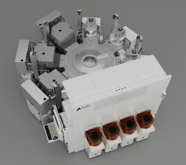
Production and supply from global production bases in Korea
Lam Research is supporting advanced logic and memory semiconductor development solutions with its portfolio of high-selectivity etching equipment featuring innovative etching technologies and chemistry solutions.
Lam Research today announced a family of high-selectivity etch products that support the development of gate-all-around (GAA) transistor structures by applying innovative wafer manufacturing technologies and new chemistry solutions.
Lam Research's portfolio of high-selectivity etching equipment, comprised of three new products: Argos®, Prevos™, and Selis®, provides powerful design and process advantages for advanced logic and memory semiconductor development.
These devices are produced at Lam Research Manufacturing Korea, Lam Research's global production base in Korea.
Lam Research's high-selectivity etch solutions provide the ultra-high selectivity and non-damaging film quality required to support the formation of advanced logic structures such as nanosheets and nanowires. It is a key technology that supports an innovative leap from planar structures to 3D structures when the integration limit is reached in the semiconductor manufacturing process.
Developed in collaboration with the world's most innovative logic and foundry semiconductor manufacturers, Lam's high-selectivity etch technology is already used in nearly a dozen key steps in the advanced logic wafer development process by industry leaders such as Samsung Electronics.
“The semiconductor industry is constantly evolving to deliver more powerful and faster device performance. As device density and complexity increase dramatically, selective etching technology is a critical enabler for manufacturing cutting-edge logic device technologies,” said Master Bae Keun-hee of Samsung Semiconductor Research Institute. “With rapidly growing global demand for our technology, we need extensive innovation and capabilities in selective etching to increase production and accelerate our logic device roadmap for GAA devices and beyond.”
Lam Research's high-selectivity etch equipment portfolio consists of three new devices.
Equipped with the innovative MARS™ (Metastable Activated Radical Source) technology, Argos provides groundbreaking wafer surface treatment and contamination removal technologies to achieve optimized semiconductor performance.
Prevos' novel etching gas and innovative vaporization technology, along with rapid temperature control, enable ultra-high selectivity etching of oxide and metal films at the atomic layer level. Prevos utilizes new etching gases developed exclusively by Lam Research, and can be expanded to support semiconductor manufacturers' production needs.
Selis adopts unique radical and high-temperature etching capabilities to provide uniform etching from top to bottom without damaging the wafer surface structure, enabling ultra-high selective etching.
Prevos and Selis provide production flexibility by configuring multiple devices in a single system, enabling selective multi-layer etching and minimizing waiting time between processes.
“Lam Research is driving the wafer fabrication advancements needed to support the semiconductor industry’s move to 3D architectures and make next-generation digital technologies a reality,” said Tim Archer, Lam Research’s chairman and chief executive officer. “For more than 40 years, Lam has driven industry innovation in etch, and we are proud to continue that legacy with the introduction of a new family of cutting-edge, innovative high-selectivity etch solutions for advanced logic and memory, available in the market today.”

Comments
Related news
Lam Research Doubles Domestic Production Capacity… Establishes New Hwaseong Plant
Lam Research Manufacturing Korea is doubling domestic production capacity through the establishment of a new Hwaseong facility and providing one step ahead of support to semiconductor customers worldwide.
2021.11.01by 배종인 기자
Lam Research Implements 300mm Wafer Deep Silicon Etching
Lam Research is expanding its Deep Silicon Etch technology and launching new etching equipment capable of producing devices on 300mm wafers, making a full-scale push to support chip development for automotive and smart technology applications.
2021.12.10by 배종인 기자
Lam Research Discusses Next-Generation Semiconductor Technology at Semicon Korea
Global semiconductor equipment manufacturer Lam Research Corporation, which supplies wafer fabrication equipment and services, will discuss next-generation semiconductor technology at Semicon Korea 2022.
2022.02.07by 배종인 기자

Intel Unveils Next-Generation 'Core Ultra Series 3' and vPro Platform for Enterprise PCs
Intel has officially unveiled the "Intel Core Ultra Series 3" for next-generation enterprise PCs and the latest vPro platform, addressing a wide range of demands from enterprise notebooks to high-performance workstations.
2026.03.26by 배종인 기자

ROHM Launches ESD Protection Diode Compatible with High-Speed Interfaces of 10Gbps or Higher
Semiconductor specialist ROHM has developed the 'RESDxVx series' of ESD (electrostatic discharge) protection diodes capable of responding to next-generation high-speed data communication environments exceeding 10Gbps, simultaneously enhancing both signal quality maintenance required in high-speed interfaces and IC protection performance.
2026.03.26by 배종인 기자











