



Applied Technologies, 2D EUV Process Miniaturization & New 3D GAA Technology
 Published2022.04.28 14:02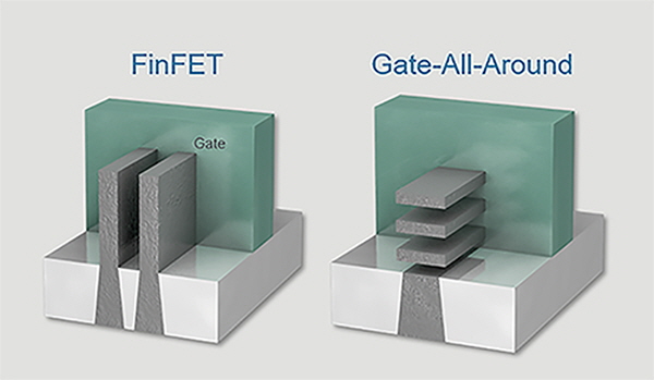
Extensive portfolio including two new IMS systems
Applied Materials has driven the expansion of 2D process miniaturization and the improvement of 3D GAA transistor engineering technology through new technology.
Applied Materials announced on the 28th innovative technologies that enable customers to continue 2D process miniaturization with EUV (extreme ultraviolet) and a technology portfolio for manufacturing next-generation 3D GAA (Gate All Around) transistors.
Applied's newly unveiled 'Stensar Advanced Patterning Film' for EUV is deposited using Applied's 'Precision CVD' system.
Unlike spin-on deposition, Applied's CVD films can control the EUV hardmask layer thickness and etching characteristics.
If semiconductor manufacturers use this film, they can achieve near-perfect EUV pattern transfer uniformity across the entire wafer.
Applied also introduced the 'Sym3 Y' etching system. With the Sym3 Y etching system, customers can perform thin film etching and deposition in the same chamber, allowing them to improve EUV patterns before etching the wafer.
The Sym3 chamber redeposits thin films in a unique manner that smoothly removes EUV resist material and then normalizes it by compensating for pattern variability caused by 'stochastic errors'.
Improved EUV patterns increase yield and enhance semiconductor power and performance. Based on this Applied Sym3 technology, the company is growing rapidly not only in the memory sector but also in the logic and foundry fields.
Currently, Applied is the number one supplier of conductor etching systems in the DRAM memory market.
Applied also developed the 'IMS' system for gate oxide stacks.
As the gate oxide thickness decreases, the driving current and transistor performance increase. On the other hand, leakage current also increases at the same time, resulting in power waste and heat generation.
Applied's newly released IMS system reduced oxide thickness to 1.5 angstroms (a unit of length used to measure the distance between atoms, 1 angstrom = 0.1 nanometer) compared to the previous method.
Through this, semiconductor companies can increase performance without increasing gate leakage, or reduce gate leakage by more than one-tenth while maintaining performance.
This IMS system integrated atomic layer deposition (ALD), heat treatment, plasma treatment, and measurement into a single high-vacuum system.
Applied also introduced an IMS system for GAA metal gate stack engineering.
If customers use this system, they can tune the threshold voltage by adjusting the gate thickness.
This enables the implementation of computing performance required in various fields, ranging from mobile devices to high-performance servers.
This IMS system performs the process under a high vacuum, minimizing contamination caused by exposure to the atmosphere.
"Applied Materials' strategy is to become a company that realizes PPACt for its customers," said Prabu Raja, Vice President and General Manager of the Semiconductor Products Group at Applied Materials. "We have unveiled seven innovative technologies that enable customers to continue 2D process miniaturization with EUV."
In addition, “GAA transistors are manufactured in a fundamentally different way from today’s FinFET transistors.” “Applied has developed two new Integrated Materials Solutions (IMS) for the realization of ideal GAA gate oxides and metal gates, and announced a wide range of products for GAA manufacturing, including epitaxy, atomic layer deposition, and selective thin film removal processes,” he said.

Comments
Related news

Applied Introduces Case Study of Continuous Chip Scaling Innovation
Applied Materials Korea, a global leader in materials engineering solutions (CEO Mark Lee), presents innovative chip expansion cases through PPACt improvement at Semicon Korea.
2022.02.08by 배종인 기자

Applied Earns Record Quarterly Performance in Q1
Applied Materials, a global leader in materials engineering solutions, achieved record quarterly results in the first quarter of 2022 driven by market strength for supply chain expansion.
2022.02.18by 배종인 기자

Applied Proves Strengthening Partnership with Intel
Intel, pursuing a restructuring of the global materials, components, and equipment supply chain through aggressive semiconductor facility investments, has achieved results demonstrating strengthened partnership with Intel among global supply chain partners, particularly with Applied Materials.
2022.04.12by 명세환 기자

Intel Unveils Next-Generation 'Core Ultra Series 3' and vPro Platform for Enterprise PCs
Intel has officially unveiled the "Intel Core Ultra Series 3" for next-generation enterprise PCs and the latest vPro platform, addressing a wide range of demands from enterprise notebooks to high-performance workstations.
2026.03.26by 배종인 기자

ROHM Launches ESD Protection Diode Compatible with High-Speed Interfaces of 10Gbps or Higher
Semiconductor specialist ROHM has developed the 'RESDxVx series' of ESD (electrostatic discharge) protection diodes capable of responding to next-generation high-speed data communication environments exceeding 10Gbps, simultaneously enhancing both signal quality maintenance required in high-speed interfaces and IC protection performance.
2026.03.26by 배종인 기자











