


Ionic PVD Systems Provide Solutions for 2D Process Miniaturization Wiring Problems
 Published2022.06.08 15:46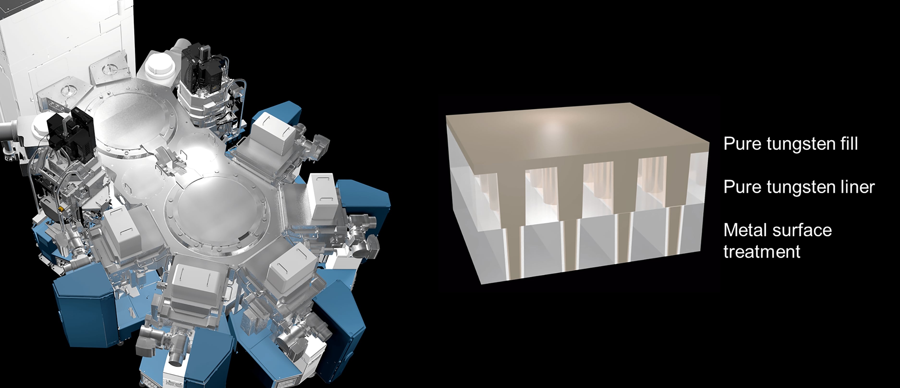
Applied Materials Ionic PVD System
Semiconductor manufacturers are using advanced lithography technologies to scale chips down to the 3nm node and below. However, as line widths become thinner, electrical resistance increases dramatically. This results in reduced semiconductor chip performance and higher power consumption, negating the benefits of advanced transistors. To address this metal wiring resistance, a new solution has emerged.
Applied Materials announced on the 8th a new system that reengineers transistor metallization to significantly reduce electrical resistance, a key bottleneck in improving chip performance and power.
Chip metallization is deposited within trenches and vias etched into a dielectric material. Conventionally, this metallization is deposited using a metal stack, which includes: a barrier layer to prevent metal from mixing with the dielectric; a liner layer to promote bonding; a seed layer to facilitate metal injection; a metal such as tungsten or cobalt used for transistor electrodes; and copper for interconnect wires.
Unlike trenches and vias, barriers and liners are not as finely detailed, which reduces the space available for conductive metal. Also, as the metal wiring becomes finer, the electrical resistance increases.
Ionic PVD allows semiconductor manufacturers to replace high-resistivity liners and barrier layers made of titanium nitride with 100% pure, low-resistivity PVD tungsten thin films, which can then be combined with CVD tungsten to create 100% pure tungsten metal electrodes. This solution addresses resistance issues and enables 2D process scaling to the 3nm node or below.
The Ioniq PVD System is Applied's Integrated Materials Solution (IMS) that supports PVD (physical vapor deposition) and CVD (chemical vapor deposition) processes, as well as surface treatment processes, in a single high-vacuum system.
“Applied’s latest innovation in solving electrical resistance is a great example of how materials engineering is enabling continued 2D scaling,” said Prabhu Raja, vice president and general manager of the Semiconductor Products Group at Applied Materials. “Our innovative Ionic PVD system eliminates bottlenecks that slow transistor performance, enabling faster transistor operation and reduced power loss.”
“As semiconductors continue to become more complex, the ability to integrate multiple processes under high vacuum conditions is becoming increasingly important for innovation in metallization to help customers achieve their high-performance and low-power goals,” he said.
Meanwhile, more information about Applied Materials' solutions for solving metallization and interconnection challenges, including the Ionic PVD system, can be found in the masterclass, "New Methods for Semiconductor Metallization and Integration."

Comments
Related news
Applied Technologies, 2D EUV Process Miniaturization & New 3D GAA Technology
Applied Materials has driven expansion of 2D process miniaturization and enhancement of 3D GAA transistor engineering technology through new technologies.
2022.04.28by 배종인 기자

Applied Materials' second-quarter sales reached $6.25 billion.
Applied Materials announced its fiscal year 2022 second quarter results on the 19th local time. Applied Materials' global revenue for the second quarter was $6.25 billion on a U.S. GAAP basis, with a gross margin of 46.9%. Operating income and operating margin were $1.89 billion and 30.3%, respectively, while earnings per share (EPS) reached $1.74.
2022.05.20by 명세환 기자

Applied Materials Leads the Way in Protecting a Sustainable Environment
Applied Materials Korea took the lead in creating a sustainable environment through education and practice to improve water quality in national rivers in the southern Gyeonggi region.
2022.05.30by 배종인 기자

Intel Unveils Next-Generation 'Core Ultra Series 3' and vPro Platform for Enterprise PCs
Intel has officially unveiled the "Intel Core Ultra Series 3" for next-generation enterprise PCs and the latest vPro platform, addressing a wide range of demands from enterprise notebooks to high-performance workstations.
2026.03.26by 배종인 기자

ROHM Launches ESD Protection Diode Compatible with High-Speed Interfaces of 10Gbps or Higher
Semiconductor specialist ROHM has developed the 'RESDxVx series' of ESD (electrostatic discharge) protection diodes capable of responding to next-generation high-speed data communication environments exceeding 10Gbps, simultaneously enhancing both signal quality maintenance required in high-speed interfaces and IC protection performance.
2026.03.26by 배종인 기자











