


SK Hynix to mass produce world's highest 238-layer NAND in the first half of next year
 Published2022.08.03 06:30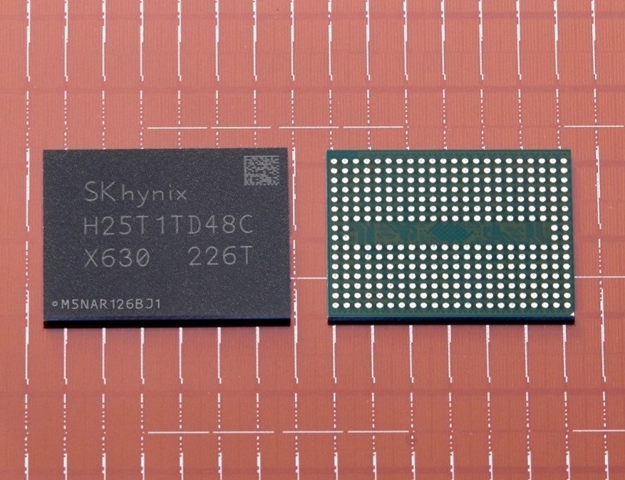
▲SK Hynix 238-layer 512-gigabit TLC (Triple Level Cell) 4D NAND flash (Photo-SK Hynix)
Improve productivity, speed, and power consumption by implementing the highest-level, smallest-area products
The era of 200-layer NAND is dawning. As competition among NAND flash semiconductor companies intensifies, the competition for the highest layer of vertically stacking cells is taking place in the 200-layer range.
SK Hynix has succeeded in developing the highest-level 238-layer NAND. On the 3rd, SK Hynix released samples of the 238-layer 512-gigabit TLC (Triple Level Cell) 4D NAND flash to customers and announced plans to begin mass production in the first half of next year.
SK Hynix has proven its technological prowess by successfully implementing 238 layers, which is higher than the world's first 232-layer NAND flash from Micron in the US last month.
SK Hynix unveiled a new product at the 'Flash Memory Summit (FMS) 2022', the world's largest NAND flash industry conference that opened in Santa Clara, USA on this day. In the event keynote speech, Choi Jeong-dal, SK Hynix Vice President in charge of NAND development, emphasized, “SK Hynix has secured global top-class competitiveness in terms of cost, performance, and quality through the development of 238-layer 4D NAND technology,” and “We will continue to innovate to overcome technological limitations.”
In this year’s event keynote, SK Hynix made a joint presentation with its NAND solutions subsidiary, Solidigm.
SK Hynix has been introducing 4D products that go beyond the existing 3D since the 96-layer NAND developed in 2018. To create 4D, where chips are implemented in a four-dimensional structure, the company’s engineers applied CTF (Charge Trap Flash) and PUC (Peri Under Cell) technologies. 4D has the advantage of increasing production efficiency while reducing the cell area per unit compared to 3D.
Not only does the 238-layer process have a higher number of layers, but it is also the world’s smallest, which increases productivity by 34% compared to the previous generation of 176 layers. This is because more chips with larger capacities per unit area are produced per wafer than before.
In addition, the 238-stage data transfer speed has increased by 50% compared to the previous generation to 2.4Gb per second. In addition, the energy usage of the chip when reading data has decreased by 21%, so it is expected to meet the 'power-to-performance' trend by reducing power consumption.
SK Hynix announced that it plans to first supply the 238-layer product that goes into cSSD (client SSD), a PC storage device, and then expand the product's utilization range to high-capacity SSDs for smartphones and servers. Next year, a 1Tb product with twice the capacity of the current 512Gb will also be introduced.
SK Hynix said, “We have succeeded in developing next-generation technology just 1 year and 7 months after developing 176-layer NAND in December 2020,” adding, “This 238-layer NAND is particularly significant in that it is the world’s smallest product while being the highest layer.”

Comments
Related news

SK Hynix Selects DITi as 6th Generation Technology Innovation Enterprise
SK Hynix has selected DITi Co., Ltd. as its 6th generation technology innovation enterprise, expanding the scope of co-growth with SK Hynix over two years, including support for equipment technology development.
2022.07.20by 배종인 기자
SK Hynix, Q2 13.811 trillion won… All-time quarterly record
SK Hynix achieved record-breaking quarterly results in the second quarter of 2022, driven by increased NAND prices and overall sales volume growth, despite the decline in DRAM prices.
2022.07.27by 배종인 기자
.png)
SK Hynix Completes Acquisition of Key Foundry
SK Hynix is completing its acquisition of Kifoundry and is now moving in earnest to expand its foundry ecosystem following its memory business.
2022.08.02by 배종인 기자

Intel Unveils Next-Generation 'Core Ultra Series 3' and vPro Platform for Enterprise PCs
Intel has officially unveiled the "Intel Core Ultra Series 3" for next-generation enterprise PCs and the latest vPro platform, addressing a wide range of demands from enterprise notebooks to high-performance workstations.
2026.03.26by 배종인 기자

ROHM Launches ESD Protection Diode Compatible with High-Speed Interfaces of 10Gbps or Higher
Semiconductor specialist ROHM has developed the 'RESDxVx series' of ESD (electrostatic discharge) protection diodes capable of responding to next-generation high-speed data communication environments exceeding 10Gbps, simultaneously enhancing both signal quality maintenance required in high-speed interfaces and IC protection performance.
2026.03.26by 배종인 기자











