This page was machine-translated and may differ from the original. View original

LG Innotek unveils new FC-BGA substrates at KPCA show 2022.

Google 우선 소스Published2022.09.20 08:49

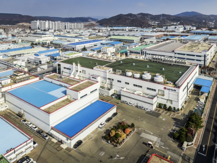
▲A panoramic view of LG Innotek's Gumi plant. In July, LG Innotek announced plans to invest 1.4 trillion won, including building a new FC-BGA production line at its Gumi Plant 4, with the goal of mass production next year. (Photo: LG Innotek)
Display of global leading products, including radio frequency package substrates and chip-on-film.

Despite the recent overall downturn in the components market, the semiconductor substrate market remains strong. With positive forecasts for long-term semiconductor demand prevailing, domestic industry expansion in semiconductor post-processing is expected.
LG Innotek will participate in the 'International PCB & Semiconductor Packaging Industry Exhibition (KPCA show 2022)' held at Songdo Convensia in Incheon from September 21 to 23 and showcase new substrate material products.
'KPCA Show 2022' is an international PCB and semiconductor packaging exhibition hosted by the Korea PCB and Semiconductor Packaging Industry Association (KPCA). About 180 domestic and foreign companies will participate to share the latest technology trends.
At the opening ceremony on the first day, LG Innotek President Jeong Cheol-dong, who is also the president of the KPCA, is scheduled to give an opening address.
At this exhibition, LG Innotek will unveil innovative products in three fields: ‘Flip Chip Ball Grid Array (FC-BGA) substrates,’ ‘package substrates,’ and ‘tape substrates.’
FC-BGA Substrate Zone Debuts New Products
At the FC-BGA Substrate Zone, LG Innotek will unveil its new FC-BGA products, scheduled for mass production next year. FC-BGA substrates are semiconductor substrates that connect semiconductor chips to the main board. They are primarily used in central processing units (CPUs) for PCs and servers, graphic processing units (GPUs), and communication chipsets.
In particular, LG Innotek announced that it improved product performance by applying various DX technologies such as AI and digital twin to the FC-BGA development process to minimize the 'warping phenomenon' in which the substrate warps due to heat and pressure during the manufacturing process. LG Innotek explained that through AI simulation, it quickly and accurately found the optimal combination of substrate circuit material composition ratio and design structure that does not cause the 'warping phenomenon'.
As the FC-BGA substrate area continues to increase due to high performance and high specifications in PCs and servers, resolving the 'warping phenomenon' proportional to the area is a critical issue that determines the success or failure of the product. That is why the market is paying attention to LG Innotek's competitiveness.
In addition, LG Innotek emphasized that FC-BGA substrates can be manufactured in various thicknesses desired by customers depending on the application, such as coreless (core layer of semiconductor substrate removed), thin core, and thick core substrates. LG Innotek stated that the application of coreless technology, which was first applied to radio frequency system-in-package (RF-SiP) substrates, to FC-BGA substrates was effective.
Substrate Zone Showcases Ultra-Precision, Ultra-Fine, and High-Integrity Technology
The Package Substrate Zone showcases semiconductor substrates used in the latest mobile wireless communication front-end modules, application processors, and memory. The exhibit includes substrates for RF-SiP, which holds the world's leading market share, as well as substrates for flip-chip chip-scale packages (FCCSPs) and chip-scale packages (CSPs).
In particular, RF-SiP substrates, used in communications semiconductors, utilize ultra-precision, high-density technologies such as microcircuits and coreless circuits, along with new materials, to significantly reduce thickness and signal loss compared to existing products. LG Innotek added that these products not only enable more efficient design of smartphone internal space, but also maximize the transmission efficiency of 5G communication signals.
The Tape Substrate Zone will showcase Chip-on-Film (COF), which has maintained the world's No. 1 market share, as well as 2-Metal Chip-on-Film (2Metal COF) and Chip-on-Board (COB). Chip-on-film and two-metal chip-on-film connect display panels and main boards in smartphones, TVs, etc., while chip-on-board is used in credit cards, passports, etc.
Chip-on-film, which uses ultra-fine technology, is suitable for high-resolution and thin-bezel displays, and demand is rapidly increasing not only for LCDs but also for OLEDs.
Son Gil-dong, Executive Director of the Substrate Materials Division, said, “Based on our global market-leading capabilities, we will rapidly expand our substrate materials business areas from mobile and display-centered areas to PC/server, communication/network, metaverse, and automobile, and continue to introduce new substrate materials products to innovate customer experiences.”
본 기사에 대한 정정·반론·추후보도 청구는 보도 청구 안내를, 그간 게재된 보도문은 정정·반론보도 모아보기를 참고해 주세요.
명세환 기자
명세환 기자