



The Key to Semiconductor Miniaturization: 'Transistor Structure'
 Published2022.10.17 16:57
As semiconductor technology continues to develop, competition to improve performance is becoming fiercer. In order to densely integrate transistors on a limited area silicon substrate, the recent trend of process miniaturization has reached 3 nanometers. Experts unanimously say that as the miniaturization process deepens, miniaturization in the next-generation process is reaching its limit.
As diversified approaches to overcome limitations are observed across the semiconductor academia and industry, ideas for new transistor structures, such as 3D stacking technology, are emerging as next-generation technologies.
The era of 32nm Planar FET, which developed miniaturization technology by focusing on leakage current issues through high-K metal gate optimization 20 years ago, has progressed through successive generations through the current mainstream FinFET process starting from 14nm.
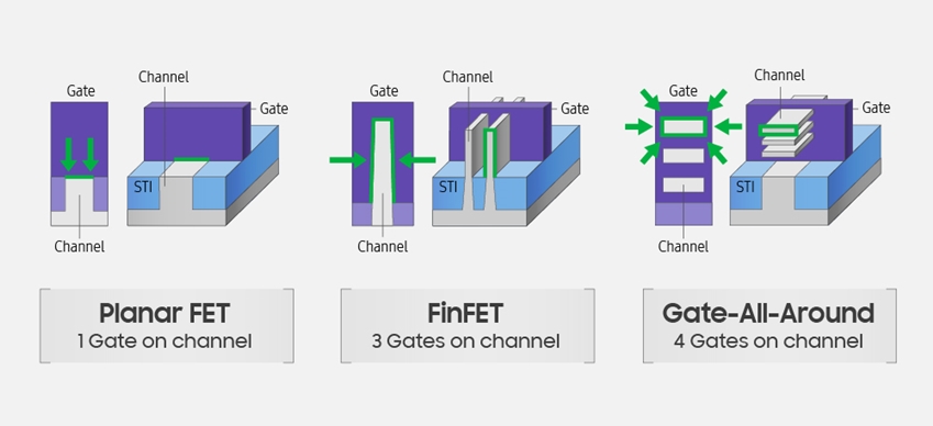
▲Semiconductor process development flow (Image-Samsung Electronics Newsroom)
Last June, Samsung Electronics succeeded in developing the world's first semiconductor using 3nm GAA (Gate All Around) technology. Starting with 3nm, the era of MBC (Multi-Bridge Channel) FETs based on the GAA process began. The channel changed to a multi-bridge channel structure and became a thin and wide nanosheet shape. This made it possible to easily and diversely control the channel size by adjusting the nanosheet width. It is evaluated that the performance efficiency has been improved as the current can be controlled more finely compared to the existing FinFET process.
The semiconductor process, which is one step more advanced than the existing Fin FET process, has been continuously developing while looking toward the next stage.
The industry says that it takes 20 years from concept idea to commercialization in the semiconductor development process. The industry is already in the stage of anticipating and preparing for the next-generation semiconductor process. For the 2nm process and below, concepts such as vertical FET (VFET) and NC (Nagative Capacitance) FET are being proposed.
Park Jeong-won, a professor of electrical engineering at the University of Nevada, predicted at the ‘Global New Industry New Technology Seminar’ that “when semiconductor technology advances below 2 nanometers, vertical FETs, 2D new materials, and NCFETs will emerge as the next generation.”
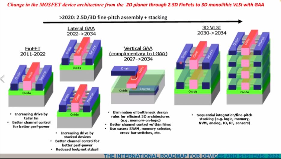
▲Semiconductor process development outlook until 2034 (Data - Capture from the Korea Industrial Technology Promotion Agency Global New Industry New Technology Seminar)
In particular, the dominant view is that the transistor structure will move toward a 3D stacking form. 3D stacking, which is limited to NAND flash, is expected to be applied to logic and memory to increase integration after 10 years. Experts predict that Lateral GAA will evolve into Vertical GAA and even 3D VLSI will emerge around 2034.
Professor Park said, “We are researching and developing a nanowire GAA-based negative capacitance GaAs/InN tunnel FET that integrates the ideas of GAA, tunnel FET, and compound semiconductors.” In response to our magazine’s question about the possibility of expanding the application of compound semiconductors to next-generation semiconductors, Professor Park said, “GaN materials can be applied as tunneling transistors,” but “the problem of large-area scaling remains a major challenge.”

Comments
Related news
Samsung's Super Gap, World's First GAA-Based 3nm Semiconductor Mass Production Begins
Ten years ago, Samsung held only about 1% of the global foundry market share, but has now narrowed the gap enough to challenge TSMC, the current foundry leader. Within five years of launching Samsung Electronics' foundry business division, the company unveiled the world's first GAA-based 3-nanometer process and is demonstrating a pace in process miniaturization that is at least one step ahead of TSMC.
2022.06.30by 명세환 기자
[Semiconductor Show 2022] CEO Kwak No-jeong: "Development of new materials to overcome memory limitations is essential."
"Innovation in 'high-K dielectric materials' must be accompanied. Development of new materials is necessary to address resistance issues resulting from contact size reduction."
2022.10.06by 명세환 기자

Samsung Electronics Unveils Memory Roadmap… Developing 10nm DRAM and 1,000-Layer NAND
"Samsung Electronics has surpassed 1 trillion gigabytes (GB) in total storage capacity of memory produced over approximately 40 years, and with half of that having been manufactured in the past 3 years, we are experiencing the rapidly transforming digital transition firsthand."
2022.10.07by 명세환 기자

Intel Unveils Next-Generation 'Core Ultra Series 3' and vPro Platform for Enterprise PCs
Intel has officially unveiled the "Intel Core Ultra Series 3" for next-generation enterprise PCs and the latest vPro platform, addressing a wide range of demands from enterprise notebooks to high-performance workstations.
2026.03.26by 배종인 기자

ROHM Launches ESD Protection Diode Compatible with High-Speed Interfaces of 10Gbps or Higher
Semiconductor specialist ROHM has developed the 'RESDxVx series' of ESD (electrostatic discharge) protection diodes capable of responding to next-generation high-speed data communication environments exceeding 10Gbps, simultaneously enhancing both signal quality maintenance required in high-speed interfaces and IC protection performance.
2026.03.26by 배종인 기자











