


[Technical contribution] Infineon Technologies - Reliability verification based on understanding the characteristics and operation of wide bandgap devices
 Published2022.11.25 12:05
■ WBG 디바이스, 라이프사이클 모델링 新 접근법 必
갈륨 나이트라이드(GaN) 및 실리콘 카바이드(SiC) 디바이스가 고유의 특성을 앞세워서 전력 전자 애플리케이션에서 실리콘을 대신해서 인기가 높아지고 있다.
SiC 디바이스는 높은 전압에서도 스위칭 손실이 낮은 유니폴라 디바이스를 가능하게 하고, GaN 디바이스는 매우 높은 주파수로 스위칭 할 수 있다.
이러한 특성들에 의해서 더 소형화되고 전력 효율이 우수한 디자인을 달성할 수 있다.
그런데 이들 기술은 비교적 최근에서야 양산이 가능해짐으로써 현장에서 장기적 성능에 관해서 알려진 정보가 많지 않다.
실리콘 디바이스는 장기간에 걸쳐서 수명 모델링이 잘 개발되어 있으므로 이를 바탕으로 신뢰성을 정확하게 예측할 수 있으나, 와이드 밴드갭 디바이스는 물리적 구조가 다르므로 디바이스 라이프사이클 모델링에 대해서 새로운 접근법을 필요로 한다.
이 글에서는 신뢰성과 관련해서 SiC 및 GaN 디바이스의 특성과 동작에 대해서 알아본다.
와이드 밴드갭 디바이스의 장기적 동작을 예측하고 현장에서 제품 수명 전반에 걸쳐서 신뢰성을 달성하도록 하기 위해서 인피니언이 개발한 프로세스와 테스트 절차에 대해서 설명한다.
■ SiC 디바이스의 특성과 결함 메커니즘
○ 게이트 산화막
SiC MOSFET은 외인성(extrinsic) 결함 밀도가 훨씬 높기 때문에, 어떠한 추가 조치를 취하지 않으면 실리콘 디바이스보다 결함 가능성이 최대 4배까지 더 높다.
게이트 산화막의 외인성 결함은 두께가 얇아지는 국부적 씨닝 현상(localized thinning effect)을 통해서 모델링할 수 있다.
이 현상으로 인해서 특정한 게이트 바이어스 전압에서 더 강한전계가 인가되어 산화막이 더 일찍 파괴될 수 있다(그림 1).
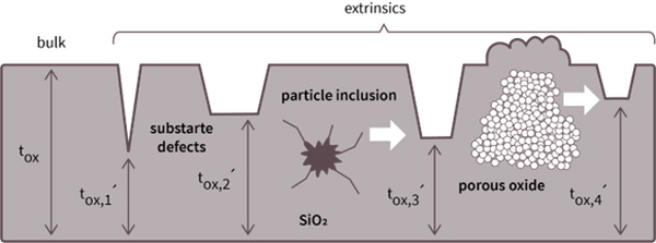
▲그림 1 : SiC 디바이스의 게이트 산화막의 국부적 씨닝 현상을 통해서 비정질 층의 외인성 결함을 수학적으로 모델링할 수 있다.
인피니언은 테스트 시에 혁신적인 검사 기법을 사용해서 잠재적으로 취약한 SiC 디바이스를 선별해서 골라낸다.
모든 디바이스에 외인성 결함이 잠재된 디바이스는 파괴되지만 결함이 없는 디바이스는 정상적으로 동작하도록 디자인된 스트레스 펄스 패턴을 가해서 테스트를 실시한다.
바이어스 온도 불안정성 또한 신뢰성에 영향을 미친다. 게이트 산화막 양단 간의 강한 전계로 인해서 디바이스 임계 전압과 결과적으로 온(on) 저항이 변화를 일으킴으로써 열 폭주가 발생될 수 있다.
정적 전압으로 인해서 발생되는 온도 불안정성에 대해서는 잘 알려져 있는데, 전이 시의 디바이스 스위칭 역시도 SiC 디바이스의 임계 전압을 변화시키는 요인으로 작용할 수 있다.
이 드리프트 양은 턴온 바이어스 전압과 스위칭 주파수에 따라서 좌우된다.
디바이스가 항상 자신의 SOA(safe operating area) 이내로 머물도록 함으로써 이러한 드리프트를 완화할 수 있기는 하다.
인피니언은 최근에 기술적으로 개선된 게이트 산화막 형성 프로세스를 도입함으로써 동적 드리프트가 임계 전압 불안정성에 미치는 영향을 크게 줄이게 됐다.
○ 바디 다이오드
SiC MOSFET의 바디 다이오드는 서브스트레이트 소재로부터 기인한 결함이 활성층(에피 층, 드리프트 영역)으로 침투함으로 인해서 바이폴라 저하가 발생될 수 있다.
그러면 드리프트 영역 내부에 스태킹 결함(stacking fault)이 성장할 수 있고, 이것은 유효 디바이스 영역을 줄이는 것으로 이어진다.
이것은 다시 시간이 경과하면서 RDS(ON)을 변화시키고 바디 다이오드의 VSD를 높이는 것으로 이어진다.
그러다가 스태킹 결함이 웨이퍼 표면에 도달하면 성장을 멈춘다(포화).
여기에 걸리는 시간은 PN 접합부를 통과하는 전류와 접합부 온도에 따라서 좌우된다.
항복 전압, 누설 전류, 스위칭 동작 같은 기본적인 파라미터들은 영향을 받지 않는다.
인피니언은 스태킹 결함 형성을 억제하도록 공정 프로세스를 최적화했다.
위에서 언급한 기술적 조치들에 더해서 완성품 디바이스로 추가적인 검사 테스트를 적용해서 스태킹 결함이 진행되고 있는 디바이스를 골라낸다.
그럼으로써 SiC 디바이스가 데이터시트 한계를 위반하지 않으면서 장기적으로 동작하도록 한다.
○ 우주 방사선(cosmic ray)
차단 모드 시에 전력 디바이스는 강한 내부 전계하에 동작한다.
SiC는 이 전계가 실리콘보다 10배 가까이 더 높다. 우주 방사선(cosmic ray)에서 유래한 입자는 지구의 대기에 영구적으로 존재하는데, 이 입자가 전력 디바이스의 활성 영역으로 침투해서 국부적인 캐리어 증식 현상을 발생시킬 수 있으며 종국에는 디바이스를 파괴시킬 수 있다.
이것을 단일 이벤트 번아웃(Single Event Burnout)이라고 한다. 베이스 층의 두께를 높이고 도핑을 줄여서 특정한 역 바이어스 전압에서의 SEB에 대한 견고성을 높일 수 있다.
하지만 이렇게 하면 더 높은 애버랜치 항복 전압을 가능하게 하는 대신에, 온(on) 상태 손실을 높인다는 함정이 숨어 있다.
우주 방사선으로 인한 결함 비율은 고도가 높아짐에 따라서 기하급수적으로 증가한다.
그러므로 인가전압, 고도, 필요한 수명 등을 비롯해서 특정 애플리케이션의 필요에 따라서 계산을 해야 한다.
인피니언의 숙련된 애플리케이션 엔지니어들이 테스트 데이터, 애플리케이션 세부사항, 미션 프로파일 등을 토대로 해서 전반적인 결함 비율을 계산하는 것을 돕는다.
또한 인피니언은 주요 목표 애플리케이션에 대한 최악 상황 미션 프로파일을 기반으로 결함 비율 요구사양을 충족하도록 디바이스를 설계한다.
○ 견고성 검증
인피니언은 SiC 기반 전력 디바이스에 대해 25년 넘게 쌓은 경험과 JEDEC 국제 표준 같은 다수의 표준 기구에 참여한 경험을 바탕으로 품질 보증 프로그램을 개발했다.
이 접근법은 욕조(bathtub) 형태의 곡선을 사용해서 제품 라이프사이클을 기술한다(그림 2). 먼저 집중적인 선별 검사를 통해서 결함 가능성이 높은 디바이스들을 골라낸다.
최소 1,000시간 이상 모든 표준 테스트들을 실시했으며, 이 시간을 나중에는 5,000시간으로 늘렸다.
이것은 표준에서 요구하는 시간을 훨씬 상회하는 것으로서, 잠재된 EOL(end-of-life) 동작을 포착할 수 있도록 한다.
디바이스 견고성을 검증하기 위한 포괄적인 검사를 통해서 어떠한 시스템 차원의 EOL 메커니즘이 발견되지 않음으로써 모든 CoolSiC™ MOSFET이 견고성이 뛰어나다는 것을 입증한다.
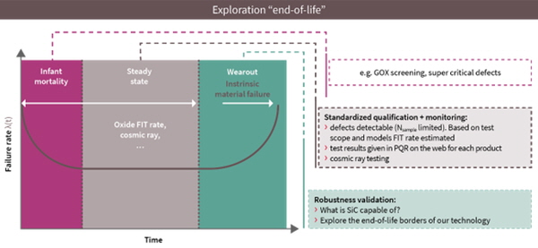
▲그림 2 : ‘욕조’ 형태의 곡선을 사용해서 전체적인 제품 수명을 기술하고 있다.

■ GaN 디바이스의 동작과 결함 메커니즘
HEMT(high electron mobility transistor) 구조를 기반으로 한 GaN 디바이스는 실리콘 기반 디바이스와 매우 다르게 동작한다.
이러한 차이 때문에 GaN HEMT 디바이스는 전력 변환 애플리케이션에서 다양한 스트레스에 대해서 실리콘보다 민감하다.
○ 애플리케이션에 따른 테스트 프로파일
이들 디바이스를 검증하기 위해서 인피니언은 애플리케이션 별로 적합한 방법으로 잠재적인 결함 모드를 검사한다.
예를 들어서 텔레콤 정류기(AC-DC) 소켓은 고온을 포함한 넓은 범위로 변화되는 주변 온도로 장시간 동작하면서 가혹한 동작 조건을 견뎌야 한다.
이 애플리케이션이 GaN 디바이스의 대표적인 활용 사례이므로, 인피니언은 이 애플리케이션을 사용해서 GaN 디바이스를 검증하기로 했다.
표 1은 2.5kW 텔레콤 정류기 시스템의 PFC(power factor correction) 디자인에서 전력 트랜지스터의 스위칭 동작을 요약해서 보여준다.
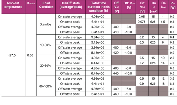
▲표 1 : 텔레콤 정류기 애플리케이션에서 디바이스 스위칭 동작(한 가지 온도에 대해서 전압과 전류 데이터)
○ 드레인-대-소스 바이어스 전압 민감성
GaN HEMT 디바이스는 공칭 정격 값 이상의 전압 및 온도 조건으로 가속 테스트했을 때 드레인-소스 바이어스 전압과 상관성이 높은 결함 비율을 나타낸다.
다시 말해서 드레인-소스 바이어스 전압이 높을수록 결함이 더 빨리 발생된다.
예를 들어서 디바이스 샘플을 800V 및 125 C로 테스트했을 때 모든 디바이스가 단 30시간 안에 결함을 나타내는데, 바이어스 전압과 온도를 낮추면 결함이 발생되기까지 걸리는 시간이 길어진다.
이러한 테스트 데이터를 사용해서 실제 사용 조건으로 결함을 예측할 수 있다.
480V 및 125 C로는 약 2백만 시간까지 결함이 발생되지 않을 것으로 예측할 수 있다(그림 3).
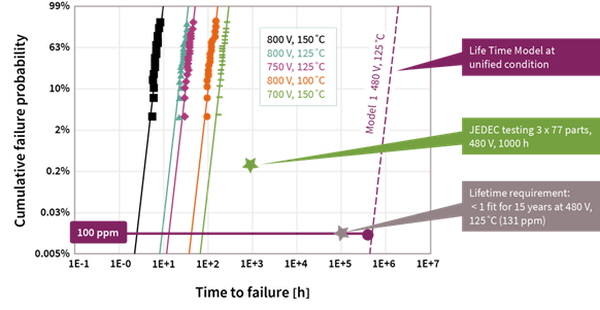
▲그림 3 : 각기 다른 DC 바이어스로 결함 시간에 따른 누적 결함 확률(왼쪽에 5개 라인)과 480V 125 C로 동작할 때 디바이스 모델(점선)
GaN 디바이스가 실리콘 디바이스보다 훨씬 더 높은 전압 스트레스를 견딜 수 있다고는 하더라도, 전압이 높을수록 수명은 감소된다.
이 모델로는 수명이 목표 요건보다 3배나 더 길다는 것을 알 수 있다. 이 그래프 상에서 초록색별은 현재 실리콘에 사용되는 검증 기법을 사용해서 감지할 수 있는 결함 확률이다(GaN 디바이스의 수명 예측에 사용하기에는 불충분).
회색별은 100ppm(parts per million)의 결함 비율 기준 15년의 목표 수명을 나타낸다.
○ 하드 스위칭
SOA 스위칭은 DHTOL(dynamic high temperature operating life)이라고도 하는 것으로서, GaN 디바이스 성능을 저하시키는 또 다른 중요한 메커니즘이다.
많은 GaN 디바이스 업체들이 장기적인 애플리케이션 스위칭 데이터를 발표하고 있다.
이것을 보면 하드 스위칭 애플리케이션에서 1,000∼3,000시간(18∼60주) 동안 디바이스가 안정적으로 동작한다는 것을 알 수 있다(일정한 케이스 온도로 측정).
반면에 이 정도의 시간으로는 수 년 간의 수명 동안 동작해야 하는 디바이스 성능에 대해서 어떠한 결론을 내리기에 불충분하다.
이에 인피니언은 장기적인 하드 스위칭 동작으로 디바이스 신뢰성을 검증하기 위해서 원래 설계된 것보다 더 높은 전압 및 전류로 디바이스를 검사하기 위한 테스트 플랫폼을 개발했다.
이 가속 스트레스 테스트는 PFC에 사용되는 것과 같은 하드 스위칭 부스트 구성으로 디바이스를 작동한다.
테스트 조건에서 디바이스에 발생되는 손상을 잘 제어해서 후속적인 결함 분석을 실시할 수 있도록 했다.
이 테스트 플랫폼은 700V에 이르는 버스 전압과 디바이스 정격 이상의 전류를 사용한다(통상적인 사용 조건은 420V).
전압과 전류가 특정한 임계를 넘으면서 디바이스들이 결함을 나타내기 시작했다.
이 정보로부터 전류, 전압, 주파수에 따른 결함 비율을 예측할 수 있는 모델을 도출했다.
그림 4는 이 모델의 결과를 스위칭 SOA 곡선으로 나타낸 것이다.
그러므로 회로 디자이너가 이것을 참고해서 이른 결함을 나타낼 수 있는 전류와 전압 조합을 피해서 디바이스를 작동할 수 있다.
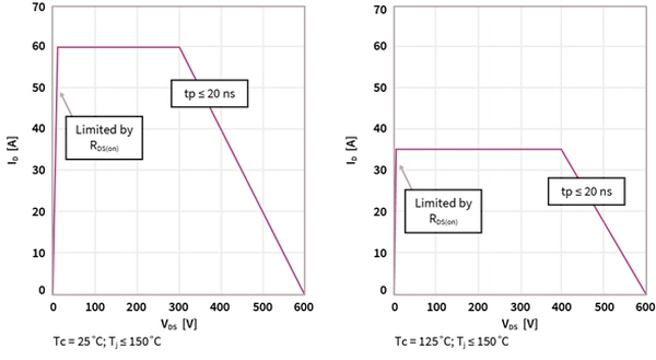
▲그림 4 : 하드 스위칭 SOA 곡선으로, 어느 구간으로 동작해야 너무 이른 결함을 피할 수 있을지 알 수 있다.
CoolGaN™ HEMT에 대해서 LLC 아키텍처를 적용한 DC-DC 컨버터에 사용되는 것과 같은 소프트 스위칭 구성으로도 가속화 테스트를 실시했다.
앞서 가속화 하드 스위칭 시에 결함이 발생되었던 동작 조건으로 (혹은 그 이상으로) 어떠한 결함이 관찰되지 않았다.
그럼으로써 스위칭 방식이 디바이스 결함에 있어서 중요한 역할을 한다는 것을 알 수 있다(그림 5).
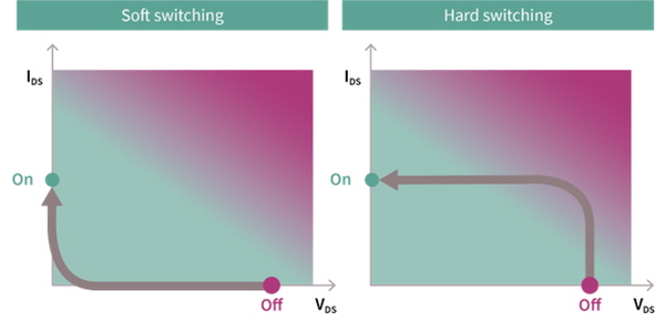
▲그림 5 : 소프트 스위칭을 사용함으로써 SOA 결함을 방지할 수 있으며, 하드 스위칭을 사용할 때는 주의가 필요하다.
■ 인피니언, WBG 디바이스 최신 정보 제공
와이드 밴드갭 디바이스(SiC와 GaN)는 비교적 최근에서야 양산이 가능해짐으로써 제품 수명 전반에 걸쳐서 신뢰성에 관한 정보가 많지 않다.
인피니언은 CoolSiC™ 및 CoolGaN™ 디바이스의 특성과 동작에 관한 깊이 있는 이해를 바탕으로 테스트 및 검증 프로세스를 개발했다.
그럼으로써 디바이스를 현장에 사용했을 때 성급하게 신뢰성과 관련한 문제를 나타내는 일이 없도록 한다.
인피니언의 와이드 밴드갭 기술 웹사이트에서 강력한 시스템 성능을 요구하는 애플리케이션 용으로 실리콘 카바이드 및 갈륨 나이트라이드 기반 디바이스 제품 포트폴리오에 관해서 더 자세한 정보를 볼 수 있다.
※ 저자
Peter Friedrichs, Vice President SiC,
Tim McDonald, Senior Director, Consulting Advisor to the CoolGaN™ program,
인피니언 테크놀로지스
※ 참고문헌
- Infineon Technologies, “How Infineon controls and assures the reliability of SiC based power semiconductors”, Whitepaper, August 2020.
- Infineon Technologies, “Reliability and qualification of CoolGaN™, Technology and devices”, Whitepaper, October 2018.

Comments
Related news
[Technical Contribution] Infineon Medic Urban & Elvir Kahrimanovic - High-Current Design Using Parallel MOSFETs for Motor Drive Applications
We have arranged a session to hear from Infineon's Medic Urban (Senior Application Engineer in Motor Drives) and Elvir Kahrimanovic (Principal Application Engineer in Motor Drives) about the importance of matching VGS(th) among parallel MOSFETs and the impact of transconductance (gfs) on current sharing.
2022.10.20by 명세환 기자

Intel Unveils Next-Generation 'Core Ultra Series 3' and vPro Platform for Enterprise PCs
Intel has officially unveiled the "Intel Core Ultra Series 3" for next-generation enterprise PCs and the latest vPro platform, addressing a wide range of demands from enterprise notebooks to high-performance workstations.
2026.03.26by 배종인 기자

ROHM Launches ESD Protection Diode Compatible with High-Speed Interfaces of 10Gbps or Higher
Semiconductor specialist ROHM has developed the 'RESDxVx series' of ESD (electrostatic discharge) protection diodes capable of responding to next-generation high-speed data communication environments exceeding 10Gbps, simultaneously enhancing both signal quality maintenance required in high-speed interfaces and IC protection performance.
2026.03.26by 배종인 기자

ST Launches 75V Drive IC Targeting 48V Industrial Motor Driving
ST Microelectronics has unveiled the 'STSPIN9P' series of 75V motor drive ICs tailored for 48V-class industrial drive system design. The new product family is characterized by half-bridge and full-bridge configurations that enable design scalability according to motor type and output conditions. Power supply circuits, protection functions, and current sensing circuits are integrated on-chip to simplify system configuration, and the devices are designed to support applications up to 500W maximum. The company plans to provide reference designs and demo boards to support development and evaluation in industrial automation, robotics, pumps, fans, lighting, and textile machinery.
2026.03.26by 배종인 기자

Nordic supports security updates for the entire lifecycle of IoT devices at a single fixed cost
Nordic Semiconductor, a global leader in low-power wireless connectivity solutions, has unveiled a single fixed-cost licensing model that delivers FOTA (Firmware Over-the-Air) and device management capabilities throughout the device lifecycle via nRF Cloud, and introduced a new firmware update solution to prepare for the enforcement of the European Union's Cyber Resilience Act (CRA).
2026.03.26by 배종인 기자











