



SK Hynix Develops Highest Capacity 24GB 12-Layer Stacked HBM3
 Published2023.04.20 10:00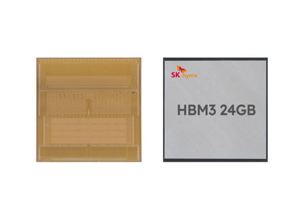
Mass production within the first half of the year, “Strengthening leadership in the cutting-edge DRAM market”
SK Hynix has set out to strengthen its leadership in the cutting-edge DRAM market by developing 'HBM3,' a 24GB 12-layer stacked DRAM with the highest performance and capacity currently available.
SK Hynix announced on the 20th that it has developed a new HBM3 product that achieves the highest capacity currently available at 24GB (gigabytes) by vertically stacking 12 individual DRAM chips for the first time in the world, and is currently verifying the product's performance with customers.
HBM (High Bandwidth Memory) is a high-value, high-performance product that 혁신적으로 boosts data processing speeds compared to conventional DRAM by vertically connecting multiple DRAMs. HBM has been developed in the order of 1st generation (HBM), 2nd generation (HBM2), 3rd generation (HBM2E), and 4th generation (HBM3).
The maximum capacity of the existing HBM3 was 16GB, which consisted of eight individual DRAM chips stacked vertically.
An official from SK Hynix emphasized, “Following the world’s first mass production of HBM3 last June, we have now succeeded in developing a 24GB package product with a capacity 50% higher than the existing one,” adding, “We expect to be able to supply the new product to the market starting in the second half of the year to meet the growing demand for premium memory driven by the recent expansion of the AI chatbot industry.”
SK Hynix's technical team applied Advanced MR-MUF and TSV technologies to this product. The company stated that it enhanced process efficiency and product performance stability through Advanced MR-MUF technology, and utilized TSV technology to vertically stack 12 individual DRAM chips that are 40% thinner than existing ones, enabling the product to achieve the same height as a 16GB product.
MR-MUF is a process of stacking semiconductor chips, injecting a liquid protective material into the spaces between the chips to protect the circuits between them, and then solidifying it. Compared to the method of laying down a film-type material every time a chip is stacked, this process is evaluated as being more efficient and effective for heat dissipation.
Through Silicon Via (TSV) is an advanced packaging technology that drills thousands of tiny holes in a DRAM chip and connects the holes of the upper and lower chips with electrodes that penetrate vertically. SK Hynix’s HBM3, which utilizes this technology, achieves a maximum speed of 819 GB/s (819 gigabytes per second), capable of transmitting 163 Full-HD movies in one second.
HBM, developed by SK Hynix in 2013 as the world's first, is attracting attention from the industry as a memory semiconductor product essential for generative AI that requires high-performance computing.
In particular, the latest standard, HBM3, is considered the optimal memory for rapidly processing large amounts of data, and demand from big tech companies is gradually increasing.
The company is currently providing HBM3 24GB samples to numerous global customers to verify their performance, and it is reported that customers are also showing great anticipation for the product.
SK Hynix Vice President Hong Sang-hoo (Head of P&T) stated, “Based on our world-class back-end process technology, we were able to successively develop ultra-high-speed, high-capacity HBM products,” adding, “We will complete preparations for the mass production of these new products within the first half of the year to solidify our leadership in the cutting-edge DRAM market for the AI era.”

Comments
Related news
.jpg)
SK Hynix Begins Mass Production of Next-Generation Memory "HBM2E"
SK Hynix has begun full-scale mass production of HBM2E. This is faster than Samsung Electronics, which announced mass production within this year, as SK Hynix achieved mass production just 10 months after developing HBM2E in August last year. SK Hynix's HBM2E is a product capable of processing 3.6 gigabits of data per second, and can handle 460 gigabytes of data per second through 1,024 I/O ports.
2020.07.03by 강정규 기자
SK Hynix Develops HBM3, the Fastest DRAM to Date
SK Hynix has developed the industry's highest-specification DRAM capable of processing data equivalent to 163 ultra-high-definition movies in just 1 second, and is expected to be utilized in high-performance data centers, machine learning, and supercomputers.
2021.10.20by 배종인 기자
[Planning-Chat GPT3③] AI Semiconductor and Data Center Market ‘Active’
Investment in key AI market infrastructure, including domestic and international AI semiconductors and data centers, is being accelerated. Samsung Electronics has been continuously advancing 'HBM-PIM,' which combines memory semiconductors and AI processors into one unit, since 2021. SK Hynix has succeeded in developing 'HBM3,' a next-generation stacked memory optimized for AI inference and learning performance. Data centers provide cloud computing services capable of collecting, storing, and analyzing big data, and are well-suited for training AI models. Domestically, investment in data centers for securing stable infrastructure is accelerating alongside AI semiconductor development.
2023.03.06by 김예지 기자

Intel Unveils Next-Generation 'Core Ultra Series 3' and vPro Platform for Enterprise PCs
Intel has officially unveiled the "Intel Core Ultra Series 3" for next-generation enterprise PCs and the latest vPro platform, addressing a wide range of demands from enterprise notebooks to high-performance workstations.
2026.03.26by 배종인 기자

ROHM Launches ESD Protection Diode Compatible with High-Speed Interfaces of 10Gbps or Higher
Semiconductor specialist ROHM has developed the 'RESDxVx series' of ESD (electrostatic discharge) protection diodes capable of responding to next-generation high-speed data communication environments exceeding 10Gbps, simultaneously enhancing both signal quality maintenance required in high-speed interfaces and IC protection performance.
2026.03.26by 배종인 기자











