


Samsung Electronics to begin mass production of 1.4nm chips and provide a one-stop AI solution by 2027
 Published2024.06.13 14:10
.jpg)
AI semiconductors in one place, from HBM to logic and optical components
Samsung Electronics will begin mass production of its 1.4nm process in 2027, integrating AI solutions with optical elements into a single package, accelerating the advancement of AI semiconductor one-stop solutions along with cutting-edge processes.
On the 12th, Samsung Electronics held the 'Samsung Foundry Forum 2024' at the Samsung Electronics DS Division America (DSA) headquarters building located in San Jose, Silicon Valley, USA.
Under the theme of 'Empowering the AI Revolution,' this event presented Samsung's unique differentiation strategy, including creating synergy through collaboration with Samsung Electronics' cutting-edge foundry technology as well as memory and advanced packaging fields to realize customers' artificial intelligence (AI) ideas.
In his keynote speech that day, Choi Si-young, President of Samsung Electronics Foundry Business, said, “At a time when all technologies are undergoing revolutionary changes centered around AI, the most important thing is high-performance, low-power semiconductors that enable AI implementation.” He added, “Samsung Electronics will provide one-stop AI solutions that customers need in the AI era through GAA (Gate-All-Around) process technology optimized for AI semiconductors and optical element technology that enables high-speed data processing with low power consumption.”quo; he said.
To meet the expanding and diversifying customer demands of semiconductor applications, Samsung Electronics is providing specialized processes for key applications, including AI, HPC, battlefield, and edge computing.
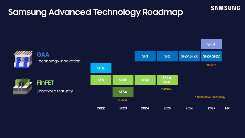
This year's event also unveiled SF2Z and SF4U, which were added to the existing foundry process roadmap.
Samsung Electronics plans to prepare a 2nm process (SF2Z) using BSPDN (Back Side Power Delivery Network) technology by 2027. BSPDN is a technology that improves the bottleneck of power and signal lines by placing the current wiring layer on the back of the wafer.
SF2Z not only improves PPA compared to the existing 2nm process, but also significantly reduces the 'voltage drop' phenomenon that causes unstable current flow, thereby improving the performance of high-performance computing designs.
PPA is an abbreviation for Power, Performance, and Area, and refers to three major indicators used in evaluating a process.
In addition, another new process announced this time, the 4nm SF4U, further enhances PPA competitiveness through optical shrink compared to the existing 4nm process, and is scheduled for mass production in 2025.
Samsung Electronics plans to mass-produce the 1.4nm process in 2027 and announced that it has achieved the target performance and yield.
To remain competitive in the 'Beyond Moore' era, we are leading future technological innovation beyond 1.4 nanometers through innovation in materials and structures.
Samsung Electronics is the first company to apply GAA transistor technology to the 3nm process and has been mass producing it since 2022, and plans to begin mass production of the second-generation 3nm process in the second half of this year.
Samsung has accumulated experience in mass production of GAA and has built up its competitiveness, and plans to continue applying this to 2nm as well. Samsung's GAA process mass production volume has been steadily increasing since 2022, and is expected to continue to expand significantly in the future due to growing demand for advanced processes.
Samsung Electronics possesses a comprehensive portfolio of foundry, memory, and advanced packaging businesses, making it advantageous for collaboration to provide customized solutions tailored to the specifications and customer needs of the AI era.
Samsung Electronics is leveraging collaboration across its three business areas to deliver integrated AI solutions that offer high performance, low power, and high bandwidth, simplifying customers' supply chains and accelerating product launches.
Fabless customers leveraging Samsung's integrated AI solutions can reduce the time from chip development to production by approximately 20% compared to using separate foundries, memory, and packaging companies.
Furthermore, by 2027, the company plans to integrate optical components into AI solutions. This is expected to provide customers with the "one-stop AI solution" they need in the AI era.
Samsung Electronics is diversifying its portfolio by customer and application to strengthen the business competitiveness of its foundry division.
By strengthening customer collaboration in the rapidly growing AI field, orders for AI products this year have grown by more than 80% compared to last year.
We are responding to diverse customer needs by providing a process portfolio that improves PPA and price competitiveness even in 8-inch foundries and mature processes.
Samsung Electronics will hold the 'SAFE (Samsung Advanced Foundry Ecosystem) Forum 2024' on the 13th (local time). This year's theme is 'AI: Exploring Possibilities and Future,' and Samsung Electronics will provide a platform for partners to share and present customized technologies and solutions for the AI era.
In particular, Siemens CEO Mike Ellow, AMD VP Bill En, and Celestial AI CEO David Lazovsky will attend and discuss the future direction of chip and system design technology required in the AI era.
This forum will host the first workshop of the 'MDI Alliance (Multi-Die Integration Alliance),' an advanced packaging consultative body launched last year.
Samsung Electronics and its MDI partners will further strengthen their partnership by discussing specific cooperation plans in depth at this workshop and concretizing comprehensive solutions for 2.5D and 3D semiconductor design.

Comments
Related news

Samsung Electronics, 2024 Q1 sales 71 trillion… 11% increase year-on-year
According to Samsung Electronics' preliminary business results for the first quarter of 2024 announced on the 5th, revenue reached 71 trillion won, an increase of 11.37% compared to the same period last year, and operating profit reached 6.6 trillion won, an increase of 931.25% compared to the same period last year.
2024.04.05by 배종인 기자
Samsung Electronics Develops Industry's Fastest LPDDR5X
Samsung Electronics has successfully developed industry-leading LPDDR5X memory with performance improved by 25% and capacity increased by 30% or more compared to previous-generation products, and is expected to be able to meet the demand for low-power, high-performance semiconductors.
2024.04.17by 배종인 기자
Samsung Electronics Stacks Industry's Highest Unit of '9th Generation V-NAND'
Samsung Electronics has commenced mass production of its '1Tb (terabit) TLC (Triple Level Cell) 9th generation V-NAND,' which achieves the highest tier count implementable with a double-stack structure, demonstrating its leadership in memory semiconductor technology.
2024.04.23by 배종인 기자

Samsung Electronics, 1Q memory market improvement, semiconductor turnaround
Samsung Electronics achieved a turnaround from semiconductor losses in the first quarter of 2024, driven by rising semiconductor memory prices and demand, as well as record first-quarter foundry orders.
2024.04.30by 배종인 기자

Samsung Electronics: "HBM testing is progressing smoothly."
Samsung Electronics announced that it is smoothly progressing tests for HBM supply with various global partners.
2024.05.24by 배종인 기자











