



ACM, ALD process qualified for 300mm semiconductor mass production
 Published2024.12.12 15:50
ACM Research, Inc. has received customer process qualification certification for its 300mm semiconductor mass production atomic layer deposition (ALD) furnace equipment, and is set to begin supplying high-quality ultra-thin film deposition equipment and expanding its customer base.
ACM announced today that its Ultra Fn A plasma-enhanced atomic layer deposition (PEALD) furnace equipment has completed process qualification certification for a Chinese semiconductor manufacturing customer.
This equipment is now in mass production.
Additionally, the Ultra Fn A thermal atomic layer deposition (ALD) furnace equipment has also successfully completed process qualification with another major Chinese customer.
Ultra Fn A furnace ALD products support various thin film deposition tasks for both thermal ALD and PEALD types, and can process more than 100 300mm wafers in batches. It includes a loading area oxygen concentration control system, an integrated gas supply system and in-situ dry cleaning capabilities.
The Ultra Fn A PEALD equipment is designed for deposition of ultra-thin silicon nitride (SiN) films, significantly improving within-wafer and wafer-to-wafer uniformity.
The Ultra Fn A thermal ALD equipment is certified for silicon carbon nitride (SiCN) thin film deposition and can precisely control the film thickness at the atomic level.
“Advanced integrated circuit (IC) manufacturing relies heavily on ultra-thin film deposition,” said David Wang, CEO of ACM Research. “Our ALD platform is a revolutionary technology that addresses the complexities of fabricating advanced 3D structures.”

Comments
Related news
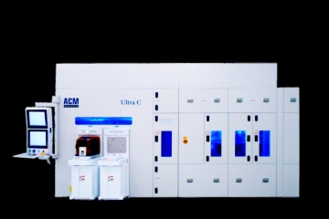
ACM Launches New Post-CMP Cleaning Equipment
Amid rising lead times in the global equipment supply chain, ACM Research is expanding its cleaning equipment portfolio by launching a new post-CMP cleaning product.
2022.08.11by 명세환 기자

ACM Launches New ALD Furnace Products
Thermal atomic layer deposition (thermal ALD) is a rapidly growing technology in advanced node processes, and as logic nodes continue to shrink, semiconductor manufacturers are intensifying their efforts to secure the latest equipment necessary for advanced processes. Against this backdrop, ACM Research has demonstrated its technological prowess by shipping advanced process equipment.
2022.10.14by 명세환 기자

ACM Enters Cotter/Developer Track Market
ACM Research, Inc., a specialist in wafer processing solutions for semiconductor and advanced wafer-level packaging (WLP) applications, has entered the semiconductor track market and begun supporting lithography for semiconductor IC manufacturing.
2022.11.25by 배종인 기자
.jpg)
ACM Research Sells Ultra C Equipment for SiC Cleaning
ACM Research, Inc., a specialist in wafer processing solutions for semiconductor and advanced wafer-level packaging (WLP) applications, has entered the power semiconductor market by securing its first purchase order for Ultra C equipment for SiC substrate cleaning.
2023.04.21by 배종인 기자
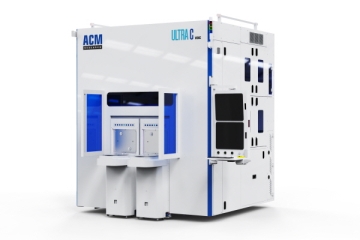
ACM Research Launches ULTRA C v Vacuum Cleaning Equipment
ACM Research, a specialized company providing wafer processing solutions for semiconductor and advanced wafer level packaging (WLP) applications, has announced a new vacuum cleaning solution that meets the new cleaning requirements of advanced 3D packages.
2023.09.27by 배종인 기자











