



Applied Materials CEO Prabhu Raja: "Collaboration through EPIC Centers will double semiconductor innovation."
 Published2025.02.25 16:12
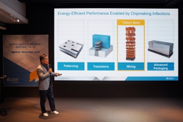
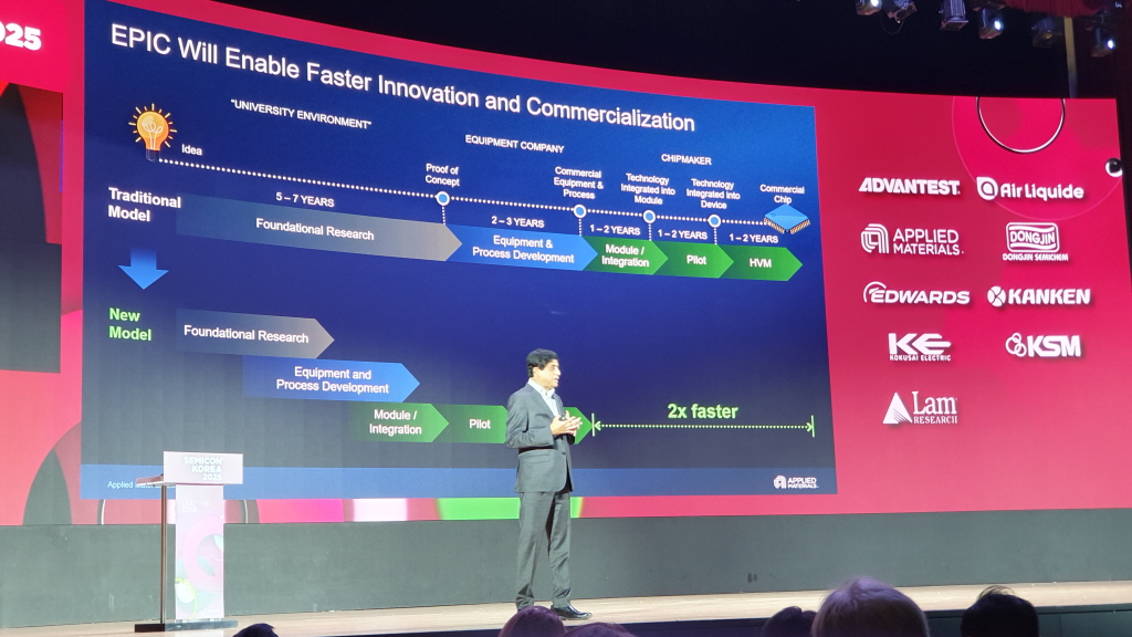 ▲Prabhu Raja, President of Applied Materials' Semiconductor Products Group, delivers a keynote speech at SEMICON Korea 2025.
Electricity demand by 2030 will increase 1,000 times, necessitating the development of technologies to reduce power consumption.
"To advance semiconductor technology, an essential element in modern industries that drives the advancement of various cutting-edge technologies, including AI and electric vehicles, integrated collaboration between industry, universities, and the government is necessary."
Prabu Raja, President of the Semiconductor Products Group at Applied Materials, gave a keynote speech at SEMICON Korea 2025 on the 19th, presenting on the topic of “Accelerating Energy-Efficient Semiconductors through Collaborative Innovation.”
Prabhu Raja said that semiconductor technology and artificial intelligence (AI) have become indispensable elements in modern industry, and that semiconductors are driving the development of various cutting-edge technologies such as AI and electric vehicles, and demand for these is rapidly increasing.
He continued by saying that AI has developed rapidly over the past 10 years, and that the case of Google's AlphaGo beating Lee Sedol, a 9-dan Go champion, is a representative example that showed the potential of AI, and that computer performance for AI model training has improved 10,000-fold over the past 5 years.
He went on to say that the development of AI technology requires a large amount of electricity, which is not sustainable, and that electricity demand is expected to reach 1,000 times the current level by 2030.
This is because AI model training requires massive data processing and complex calculations, which requires high-performance computing devices, which consume a lot of power, and power consumption is rapidly increasing because more computing resources and power are needed to make AI models more sophisticated.
This requires the introduction of new semiconductor technologies and architectures, and new approaches such as 3D semiconductor technology are required, he said.
Prabha Raja said that 3D semiconductor technology requires complexity and new materials and process technologies, and that implementing 2-nanometer technology requires more than 2,000 process steps, which require new materials and interface technologies.
In particular, he said that the method of simultaneously depositing horizontally and vertically involves extremely difficult complexities and requires highly sophisticated technology, such as precisely placing multiple materials in a very narrow space.
Additionally, new materials and process technologies are needed to address the increased contact resistance between transistors and wiring, which affects performance and power efficiency, and 20 process steps and a variety of new materials are being used, it was revealed.
He mentioned that in this process, a process is needed that integrates the existing individual processes, which can reduce resistance by 50%, and through this, the current flow can be made smoother, energy efficiency can be improved, and performance can be increased by 5%.
In addition, he mentioned that hybrid bonding technology, which combines a large number of chips into a single package, is used in 3D semiconductor technology, and that new packaging methods such as copper to copper bonding are required.
<br /> He said that for such semiconductor innovation, it is difficult for a single company to develop the technology and supply the materials, and that collaboration among various partners, including chip manufacturers, universities, and governments, is essential.
To this end, Applied Materials is building the EPIC Center, a cutting-edge semiconductor process technology and manufacturing equipment R&D collaboration facility, and stated that collaboration can be strengthened through the EPIC Center.
The EPIC Center will enable faster innovation in semiconductor technology and will double the time it takes to develop semiconductors, it claimed.
He concluded his presentation by saying that he is also preparing packaging concepts to be announced in Singapore in the future, and that he is actively promoting joint innovation with semiconductor ecosystem partners, as well as verification, market launch, and talent development.

Comments
Related news
.jpg)
Applied Achieves $6.65 Billion in Q2 Global Sales
Applied Materials recorded global net revenues of $6.65 billion for the second quarter of fiscal year 2024 under U.S. GAAP, with a gross margin of 47.4%. Operating income and operating margin were $1.91 billion and 28.8%, respectively, and earnings per share (EPS) reached $2.06.
2024.05.17by 배종인 기자
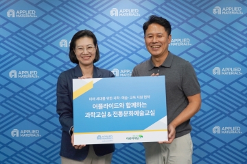
Applied, Green Umbrella Foundation and Community Science, Culture and Arts Support
Applied Materials Korea, a global leader in materials engineering solutions (CEO Park Kwang-seon), has signed an MOU with the Green Umbrella Children's Foundation for regional community science, culture, and arts education, and will sponsor the programs "Science Class with Applied Materials" and "Traditional Culture Class with Applied Materials."
2024.06.24by 배종인 기자
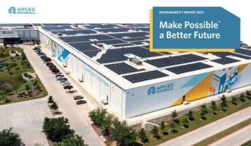
Applied to source 100% of U.S. electricity from renewable sources
According to the "2023 Sustainability Report" recently announced by Applied Materials, a global leader in materials engineering solutions, the company has demonstrated significant achievements in carbon emission reduction, including sourcing 100% of its power consumption in the United States and 70% of its global power consumption from renewable energy sources.
2024.07.01by 배종인 기자
Applied, 3Q global sales $6.78 billion… 5% increase year-on-year
Applied Materials recorded exceptional results exceeding expectations in its third quarter fiscal year 2024, ended July 28, driven by the semiconductor market boom resulting from AI leadership competition.
2024.08.21by 배종인 기자
Applied, “Ru utilization reduces power consumption by 25% and reduces gap resistance, innovating semiconductor processes below 2nm”
Applied Materials has disclosed that it is already supplying semiconductor manufacturers with technology that utilizes ruthenium (Ru), which has been frequently discussed in research stages, in mass production processes to reduce power consumption by 25% and lower void resistance, enabling application to advanced semiconductor processes of 2 nanometers and below. This announcement has raised expectations that innovation in ultra-fine semiconductor manufacturing processes will accelerate going forward.
2024.10.14by 배종인 기자











