



Ansys, Intel 18A Process Power and Electromagnetic Integrity Certification
 Published2025.05.09 13:12
.jpg)
▲3D simulation of an interposer connecting a high bandwidth memory (HBM) module to a die using Ansys HFSS IC
Global simulation company Ansys is expected to play a key role in ensuring the reliability of next-generation semiconductor systems through power and electromagnetic integrity certification of Intel's 18A process.
Ensys has obtained thermal and multi-physics verification tool certification required for semiconductor design using Intel 18A (1.8nm) process technology.
This certification plays a critical role in ensuring the reliability of next-generation semiconductor systems such as AI chips, GPUs, and high-performance computing (HPC).
ANSYS and Intel Foundry have jointly developed a comprehensive multi-physics validation analysis flow supporting Embedded Multi-Die Interconnect Bridge (EMIB) and EMIB-T technologies.
This will enable more effective support for the implementation of 3D integrated circuit (3D-IC) systems.
Ansys' flagship solutions, Ansys RedHawk-SC™ and Ansys Totem™, provide power integrity and reliability analysis capabilities based on Intel's Gate-All-Around (GAA) transistor RibbonFET and PowerVia technologies, and HFSS-IC Pro has achieved certification for electromagnetic (EM) integrity analysis of radio frequency (RF) chips and communication applications.
Additionally, ANSYS has joined the Intel Foundry Chiplet Alliance to contribute to building an interoperable chiplet design and manufacturing ecosystem.
We plan to continue our cooperation in activating Intel's 14A-E process in the future, and the Intel 18A-P process certification process is also in progress.

Comments
Related news
Intel to produce Ericsson 5G SoCs based on 18A process technology
Intel is stepping up cooperation to expand collaboration for next-generation 5G infrastructure optimization, including the production of Ericsson's 5G SoC based on 18A process technology.
2023.07.28by 배종인 기자

Ansys, Synopsys, Samsung Electronics Foundry Productivity Improvement
Ansys has launched a new reference flow for radio frequency integrated circuit (RFIC) design developed in collaboration with Sihelix for Samsung Electronics' Foundry Business Division to support the 14LPU process technology.
2023.10.16by 배종인 기자
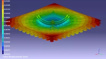
Ansys Supplies 'Thermal and Power Integrity Solution' to Samsung Foundry
Ansys Korea, a global leader in engineering simulation software (CEO Moon Seok-hwan), is closely collaborating on power and thermal management for advanced parallel (2.5D) and three-dimensional integrated circuit (3D-IC) systems, contributing to improved performance and reliability of Samsung Foundry products.
2023.10.23by 배종인 기자
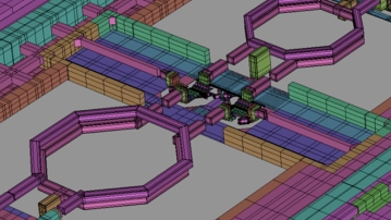
Ansys' Raptor X to Use Samsung's 8nm Design
Ansys Korea (CEO Moon Seok-hwan) announced that Samsung Electronics' Foundry Division has certified 'RaptorX', Ansys's on-chip electromagnetic (EM) design solution for ultra-high-speed product analysis, manufactured using the 8nm (nanometer) LN08LPP Low Power Plus silicon process.
2023.12.07by 배종인 기자
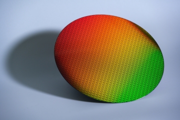
Intel Successfully Boots Operating System on 18A-Based Processor
Intel's "Panther Lake," an AI PC processor that is a flagship product based on the 18A process, and "Clearwater Forest," a server processor, have successfully booted the operating system.
2024.08.07by 배종인 기자











