



Beyond Silicon Limitations, CoolGaN™ Drives High-Efficiency Power Design Innovation
 Published2025.05.29 14:42
조용규 전무 “실제 설계 현장서 GaN은 이제 선택 아닌 필수”
“실리콘 기반 전력 소자의 물리적 한계는 이미 오래전부터 예고된 바 있습니다. 고효율·고전력밀도 설계가 요구되는 현장에서 더 이상 실리콘으로는 기대하는 성능을 끌어내기 어렵죠. 그래서 산업계는 자연스럽게 갈륨나이트라이드(GaN)로 눈을 돌리고 있습니다.”
다보코퍼레이션 기술본부 조용규 전무는 갈륨나이트라이드(GaN) 기술에 관하여 이같이 말하며, 실리콘의 한계를 극복할 차세대 전력소자 기술로서의 GaN의 가능성과 한계를 짚었다.
실제 지난 10년간 실리콘 기반 RGBT, MOSFET 소자는 스위칭 손실과 전도 손실 개선 측면에서 한계에 도달했으며, 전력 소자의 소형화 및 고주파화를 위한 스위칭 속도 개선 시도 역시 물리적 제약에 직면했다는 것이 그의 설명이다.
“스위칭 속도를 올리면 손실도 같이 증가하는 딜레마가 생기죠. 기존 방식으로는 해결이 안 됩니다. 그래서 와이드 밴드갭(WBG) 기술로의 전환이 불가피해졌습니다.”
인피니언의 CoolGaN™ 기술은 이러한 기술적 전환에 부응하는 대표적인 상용화 플랫폼이다. 독자적인 P-GaN 게이트 구조와 최적화된 에피택시 설계를 통해 기생 캐패시턴스를 줄이고 게이트 차지를 최소화함으로써 스위칭 손실을 획기적으로 줄였다. 결과적으로 최대 98%의 전력 변환 효율과 기존 대비 3배 이상의 전력 밀도를 달성할 수 있다.

조 전무는 설계자 입장에서 GaN의 장점을 극대화하기 위한 핵심 체크 포인트도 강조했다.
“단순히 소자만 바꾸면 되는 게 아닙니다. 커먼 모드 노이즈에 대한 대응, 고주파 환경에서의 게이트 드라이버 설계, PCB 내 전류 루프 최소화 등 전체 시스템 관점에서 최적화가 이뤄져야 합니다.”
또한, 인피니언은 이처럼 까다로운 설계를 돕기 위해 다양한 GaN 디바이스 포트폴리오와 함께 데모보드, 평가 플랫폼, 설계 가이드라인을 지원하고 있다. 600V/650V 클래스의 다양한 전류용량, TO-247, TOLL 등 어플리케이션 특화 패키지를 통해 전기차, 서버, 산업용 인버터, 통신 장비 등 다양한 분야에 대응 가능하다는 점도 강점이다.
.jpg)
이번 e4ds.com 에서 개최되는 6월24일 웨비나에서는 실제 데모보드를 활용한 회로 설계 사례도 소개된다. 참석자들은 ▲게이트 드라이버 설계법 ▲고주파 최적화 PCB 레이아웃 전략 ▲노이즈 억제를 위한 측정 환경 셋업법 등에 대해 실용적인 내용을 확인할 수 있다.
끝으로 조용규 전무는 GaN 기술은 기존 실리콘과는 완전히 다른 세계이며, 단순 대체가 아닌 새로운 설계적 접근이 필요하다고 강조하였다. 그러나 엔지니어 입장에서의 변화는 매우 두려운 부분이다. 하지만 이미 충분히 검증된 구조와 실전 자료들이 있으며, 이를 바탕으로 시도한다면 누구든지 빠르게 적응할 수 있을거라 조용규 전무는 말했다.
한편, 인피니언은 CoolGaN™ 기술을 통해 고효율·소형 전력 솔루션 시장에서의 리더십을 더욱 강화하고 있으며, 국내 설계자 대상 지원도 확대해나갈 예정이다.

Comments
Related news
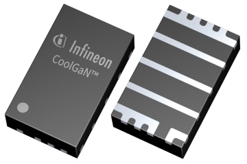
Infineon Revolutionizes Industry with GaN Transistors with Integrated Schottky Diodes
Infineon Technologies (Korea Representative Lee Seung-soo) has unveiled the industry's first CoolGaN™ G5 series of industrial GaN (gallium nitride) power transistors with integrated Schottky diodes, introducing new technology to reduce the complexity of power system design and maximize efficiency.
2025.04.18by 배종인 기자
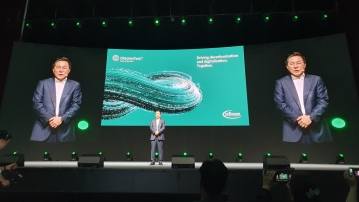
Infineon Seeks Sustainable Solutions for Global Collaboration through 'Octobertech'
Infineon Technologies held OktoberTech Seoul 2025 at COEX in Samseong-dong, Seoul on the 22nd. Andreas Urschitz, CMO, delivered the keynote speech on the theme of "Driving decarbonization and digitalization. Together." He stated that for sustainability, Infineon is developing advanced semiconductor solutions that maximize energy efficiency, and in particular, gallium nitride (GaN) and silicon carbide (SiC) based power semiconductors minimize energy loss during power conversion and play an important role in the electric vehicle, renewable energy, and industrial automation sectors.
2025.05.23by 명세환 기자

Intel Unveils Next-Generation 'Core Ultra Series 3' and vPro Platform for Enterprise PCs
Intel has officially unveiled the "Intel Core Ultra Series 3" for next-generation enterprise PCs and the latest vPro platform, addressing a wide range of demands from enterprise notebooks to high-performance workstations.
2026.03.26by 배종인 기자

ROHM Launches ESD Protection Diode Compatible with High-Speed Interfaces of 10Gbps or Higher
Semiconductor specialist ROHM has developed the 'RESDxVx series' of ESD (electrostatic discharge) protection diodes capable of responding to next-generation high-speed data communication environments exceeding 10Gbps, simultaneously enhancing both signal quality maintenance required in high-speed interfaces and IC protection performance.
2026.03.26by 배종인 기자

ST Launches 75V Drive IC Targeting 48V Industrial Motor Driving
ST Microelectronics has unveiled the 'STSPIN9P' series of 75V motor drive ICs tailored for 48V-class industrial drive system design. The new product family is characterized by half-bridge and full-bridge configurations that enable design scalability according to motor type and output conditions. Power supply circuits, protection functions, and current sensing circuits are integrated on-chip to simplify system configuration, and the devices are designed to support applications up to 500W maximum. The company plans to provide reference designs and demo boards to support development and evaluation in industrial automation, robotics, pumps, fans, lighting, and textile machinery.
2026.03.26by 배종인 기자











