


“VECTOR® TEOS 3D Presents a New Paradigm for Advanced Packaging in the AI Era”
 Published2025.11.14 11:30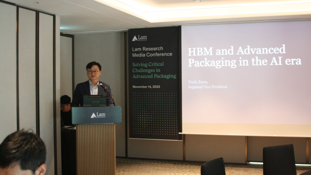
Park Jun-hong, General Manager of Lam Research Korea, is giving a speech.
Various chips, including complex logic, memory, and silicon photonics, are integrated into a single package.
In the AI era, advanced packaging is a key factor that will determine the future of the semiconductor industry in terms of performance, power, and cost. Lam Research will present a new paradigm for the semiconductor industry in the AI era through its VECTOR® TEOS 3D portfolio.
Lam Research held a media conference on the 14th and announced the 'Lam Research Advanced Packaging VECTOR® TEOS 3D Portfolio' and 'Solving Innovative Challenges in Advanced Packaging'.
First, Park Jun-hong, General Manager of Lam Research Korea, stated, “The AI revolution demands new semiconductor architectures, and now is the critical moment for advanced packaging technology to take the lead,” adding, “Accordingly, chip manufacturers are focusing on advanced packaging technology that goes beyond the chip itself.”
CEO Park Jun-hong emphasized the importance of HBM technology, stating, “HBM is a prime example of the integration of 3D stacking technology and advanced packaging. By stacking multiple memory chips vertically and connecting them via ultra-high-speed channels, it maximizes data transfer speeds and increases power efficiency.” "Recently developed next-generation products such as HBM3 and HBM4 are establishing themselves as essential technologies for AI and high-performance computing through higher stacking, higher speeds, and outstanding energy efficiency," he mentioned.
It was further reported that major Korean semiconductor companies hold a market share of approximately 75% in the global DRAM market and 56% in the NAND market, boasting world-class technological capabilities in the memory semiconductor sector. It was also stated that they are leading HBM technology, which is a key element of the AI semiconductor market, and are expanding their influence in the global memory packaging market.
In fact, the global memory packaging technology market, which is expected to reach $30.8 billion in 2025, is projected to grow at an average annual rate of 5.5% until 2030 to reach $40.3 billion.
The combination of HBM and advanced packaging plays a crucial role in overcoming the bottleneck known as the 'Memory Wall'.
This refers to the phenomenon where processors wait due to slow memory access speeds, and HBM plays a key role in the AI field, which requires large-scale parallel data processing and low latency.
HBM is establishing itself as an essential technology in various AI application fields, such as machine learning, autonomous driving, and image recognition.
In this session, innovative technologies were also introduced, including Lam Research’s advanced packaging equipment and solution portfolio, as well as the newly launched ‘Lam Research Advanced Packaging VECTOR® TEOS 3D Portfolio’.
.jpg)
Audrey Charles, Senior Vice President of Corporate Strategy and Advanced Packaging at Lam ResearchSuga is making an announcement.
Following this, Audrey Charles, Senior Vice President of Corporate Strategy and Advanced Packaging at Lam Research, gave a presentation on advanced packaging and HBM technology with the advent of the AI era.
Vice President Audrey Charles noted that the artificial intelligence (AI) revolution is causing massive changes across industries, and that advanced packaging and High Bandwidth Memory (HBM) technologies are at the center of these changes.
HBM achieves high capacity, high bandwidth, and low latency by vertically stacking multiple DRAM dies.
In this process, bump processes or hybrid bonding technologies are utilized for electrical connections between dies.
Lam Research provides key solutions for advanced packaging processes, such as etching equipment specialized for forming TSVs (Through Silicon Via) and electroplating equipment that fills TSVs with copper metal to complete electrical connections.
Currently, 12-layer stacked HBMs are being mass-produced in the industry, and expansion to 16-layer and 20-layer stacks is anticipated in the future.
Vice President Audrey Charles stated, “We will continue to innovate in the field of advanced packaging to meet the performance demands of AI computing.” The importance of advanced packaging and HBM is expected to grow even further in the future as core technologies leading the future of the semiconductor industry.
Finally, Chipping Lee, Global Advanced Packaging Technology Director at Lam Research, presented the 'Lam Research Advanced Packaging VECTOR® TEOS 3D Portfolio'.
“Advanced packaging is a core technology that enabled the AI era, and 3D heterogeneous integration technology, which stacks various types of chips (chiplets) in three dimensions beyond conventional planar (2D) integration, is essential for maximizing the performance and efficiency of AI semiconductors,” said Chipping Lee, Chief Technology Officer. “The VECTOR® TEOS 3D introduced by Lam Research is an innovative device for such 3D chiplet integration that applies proprietary deposition technology to fill minute gaps between chips without defects.”
He added, “In existing processes, there were issues with cracks or bubbles occurring when filling the gaps between chips, but VECTOR® TEOS 3D can rapidly deposit uniform and defect-free films. In particular, a major strength is the ability to deposit even thick materials flatly by introducing clamping technology that minimizes wafer warping and warpage. In fact, we succeeded in depositing 60-micron thick materials without cracks, which was considered a challenge in the industry.”
In addition, “VECTOR® TEOS is designed to integrate various chips, such as complex logic, memory, and silicon photonics, into a single package. This provides a robust process flow essential for next-generation 3D stacking technology, while simultaneously achieving high productivity and cost savings.” "We are contributing to strengthening our customers' competitiveness with deposition speeds approximately 70% faster and costs 20% lower than existing equipment," he said.
According to Chief Technology Officer Chipping Lee, this equipment has already been introduced to major logic and memory semiconductor factories around the world and has been used for mass production for over a year.
“Advanced packaging is a key factor that will determine the future of the semiconductor industry in terms of performance, power, and cost,” said Chipping Lee, Chief Technology Officer, adding, “We will continue to introduce innovative technologies in various fields such as deposition, plating, etching, and wet processes.”

Comments
Related news

Lam Research pioneers 1,000-layer 3D NAND with cryogenic etching technology
Lam Research is actively stepping forward to enable memory chip manufacturers to realize their goal of mass-producing 1,000-layer 3D NAND by 2030 through Lam Cryo™ 3.0, its third-generation cryogenic dielectric etch technology.
2024.08.01by 배종인 기자
Lam Research Invests 7 Billion Won in ‘Semiverse Solution’ to Foster Korean Semiconductor Talent
Lam Research is moving into the semiconductor megacluster in Yongin, Gyeonggi Province as the first global semiconductor equipment company, and will directly invest 7 billion won to nurture domestic semiconductor talent. The company has partnered with the Korea Semiconductor Industry Association and Sungkyunkwan University to promote semiconductor education infrastructure called the 'SemiBus™ Solution'.
2024.10.09by 배종인 기자
.jpg)
Lam Research Manufacturing Korea CEO Lee Che-soo Receives Prime Minister's Award on 'Semiconductor Day'
Lam Research Manufacturing Korea President Lee Che-soo received a commendation from the Prime Minister at the 17th Semiconductor Day commemorative ceremony, having been recognized for his contributions to strengthening the competitiveness and ecosystem of the domestic semiconductor industry.
2024.10.24by 배종인 기자

Lam Research, Semiconductor Talent Training 'Tech Academy' 2nd Class Recruitment
Lam Research Korea announced on the 12th that it is recruiting the second cohort of students for the "Lam Research Tech Academy," an initiative to nurture next-generation talent in the semiconductor industry.
2024.11.12by 명세환 기자
Lam Research, Recruiting Intern with Full-time Employment Conversion
Lam Research Korea is recruiting interns in a permanent conversion track for the Field Service Engineer (Equipment Engineer) position. Application documents can be submitted through the Lam Research Korea recruitment homepage until January 15, 2025. Final intern candidates will be selected following document screening, interviews, and a health examination.
2025.01.02by 명세환 기자











