



Applied Materials Accelerates AI Semiconductor Manufacturing Innovation
 Published2025.11.27 11:45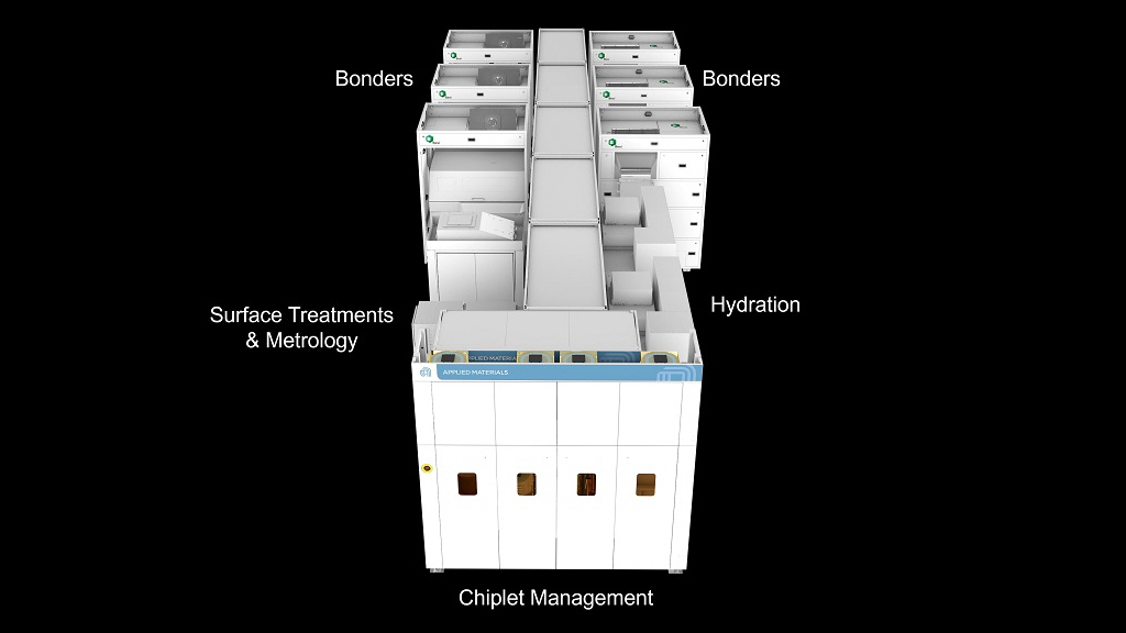
▲Applied Kinex bonding system
Centura Xtera Episystem Implements 2nm High-Performance GAA Transistors
Applied Materials, a global leader in semiconductor and display materials engineering solutions, announced next-generation semiconductor manufacturing equipment designed to maximize AI computing performance, accelerating innovation in AI semiconductor manufacturing.
On the 26th, Applied Materials introduced the Kinex bonding system, the Centura Xtera epi system, and the PROVision 10 electron beam metrology system, targeting key areas of the AI chip development competition, such as advanced logic based on GAA (gate-all-around) transistors, HBM (high-bandwidth memory) DRAM, and advanced packaging for implementing high-density 'system in package (SiP)'.
Today's GPUs and HPC chips use advanced packaging methods that combine multiple chiplets.
To support this, Applied Materials, in collaboration with Besi, has introduced the industry's first die-to-wafer hybrid bonder integrated system, Kinex.
This system improves performance and reduces power and costs through direct copper-to-copper bonding, and enhances bonding quality and consistency through process step integration. It also supports overlay measurement and drift detection with inline measurement.
Kinex systems are already in use by numerous logic, memory, and OSAT customers.
Additionally, Applied has developed the Centura Xtera epi system to form the source/drain structure that determines the performance of next-generation GAA transistors.
This system reduces gas usage by 50% with its unique low-capacity chamber structure, and improves cell-to-cell uniformity by more than 40% through the implementation of a void-free source/drain structure and deposition-etch process.
The Xtera system is being adopted by leading-edge logic and memory chip manufacturers to enhance stability and performance in sub-2nm processes.
Applied Materials also improves yields for advanced logic and memory chips with the PROVision 10 electron beam metrology system.
This system is the first in the industry to use Cold Field Emission (CFE) technology, and offers a 50% increase in resolution and a 10-fold improvement in imaging speed compared to existing systems.
It also enables 3D chip multilayer imaging and sub-nanometer precision measurements.
This system is essential for key process control, including EUV layer overlay, GAA transistor nanosheet measurement, and epi void detection.
“The proliferation of 3D architectures presents new metrology challenges,” said Keith Wells, vice president of Applied Materials. “PROVision 10 is a powerful tool for improving yields of complex chip designs.”
“As chips become more complex, we need to improve the performance and power efficiency needed to scale AI,” said Prabu Raja, president of Applied Materials’ Semiconductor Products Group.“We are focusing on innovation in materials engineering,” he said, adding, “We are working with our customers to jointly develop solutions that enable technological leaps in logic, memory, and packaging.”

Comments
Related news
.jpg)
Applied Materials' Q3 global sales reached $7.3 billion, up 8% year-over-year, achieving record sales.
Applied Materials, a leading materials engineering solutions provider for advanced semiconductors and displays worldwide, recorded record quarterly revenue of $7.3 billion in the third quarter of fiscal year 2025, which ended on July 27.
2025.08.18by 명세환 기자

Applied Intuition Launches White Box Autonomous Driving System to Understand Why Autonomous Vehicles Move the Way They Do
Applied Intuition, a global leader in vehicle intelligence, has officially launched an end-to-end autonomous driving stack solution based on advanced driver assistance systems (ADAS) that supports autonomous driving Level 2++ (L2++), thereby beginning in earnest to provide the flexibility and scalability required by manufacturers through its whitebox autonomous driving system.
2025.08.21by 배종인 기자
.jpg)
Applied Materials Launches Environmental Protection Campaign to Mark World Cleanup Day
Applied Materials Korea (CEO Park Kwang-seon) is carrying out environmental cleanup activities with employees and their families around the Dongtan Sinricheon area on the occasion of World Cleanup Day, evolving into a company that engages with the local community beyond technological innovation.
2025.09.22by 명세환 기자
Applied Materials and GlobalFoundries Partner to Develop AI-Based Photonics
Applied Materials has entered into a strategic partnership with GlobalFoundries and will establish a state-of-the-art waveguide manufacturing facility in Singapore. This collaboration is aimed at accelerating technological innovation in AI-based photonics, and the two companies plan to jointly develop high-performance optical solutions for implementing next-generation digital experiences by combining their expertise in semiconductors and materials engineering.
2025.10.02by 명세환 기자
Applied Materials Recognizes Sustainability Through ESG
Applied Materials Korea (CEO Park Kwang-seon) received both the 'Grand Prize in ESG Division' and the 'Minister of Foreign Affairs Award' at the '2025 K-ESG Management Awards' ceremony, establishing itself as a model company for sustainable management.
2025.10.22by 명세환 기자











