



Professor Kim Seong-dong of Seoul National University of Science and Technology: "'Optical Packaging' is a rapidly emerging key technology that addresses AI data transfer limitations."
 Published2025.12.19 09:44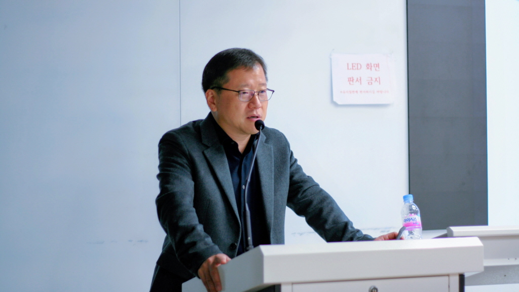
▲Professor Kim Seong-dong of Seoul National University of Science and Technology is presenting on ‘Trends in Advanced Packaging Technology.’
The next leap forward for semiconductors is packaging, a key driver of data transfer efficiency and performance in the AI era.
Optical packaging is emerging as a key technology to address data movement limitations in the AI era, establishing itself as a new competitive force in the semiconductor industry.
Professor Kim Seong-dong of Seoul National University of Science and Technology presented on 'Advanced Packaging Technology Trends' at the '2025 2nd Advanced Optical Packaging Technology Seminar' held at the Eouigwan of Seoul National University of Science and Technology on the 17th, and announced that the central axis of the semiconductor industry is shifting to 'advanced packaging'.
Professor Kim Seong-dong emphasized, “Now that Moore’s Law has reached its limits, the breakthrough for improving system performance is coming from packaging technology.”
Semiconductor manufacturing is divided into pre-process and post-process.
If the pre-process is the process of making transistors on silicon wafers, the post-process is the step of assembling and packaging them into individual chips.
Professor Kim Seong-dong said, “As the miniaturization of the entire process goes down to 3 nanometers or less, the difficulty and cost of the process have increased rapidly, making it difficult to expect performance improvements as in the past,” and “The semiconductor industry is ‘ began to change its strategy from ‘making the chips themselves fast’ to ‘making the connections between chips fast,’” he said.
Reducing the data transfer distance between the CPU and memory significantly improves system performance. To achieve this, technologies have evolved to place chips closer together, either horizontally or vertically. A prime example is 2.5D packaging, which inserts a "silicon interposer" between chips to implement fine wiring.
Professor Kim Seong-dong explained, "PCB substrates have wiring limitations of 10㎛, making them incapable of supporting ultra-fine connections between chips." Silicon interposers, however, can implement wiring as thin as 2㎛, making them ideal for connecting high-bandwidth memory (HBM) and GPUs. Indeed, NVIDIA's H100 and H200 GPUs are based on this technology.
On the other hand, as interposers become larger, cost issues have arisen again. This is due to the structural limitation that only four large interposers can be produced on a 300mm wafer.
To address this, Intel has proposed the Embedded Multi-die Interconnect Bridge (EMIB), which uses silicon only where necessary, and PCB manufacturers are also rushing to secure fine wiring technology.
Advances in packaging technology are even changing the way chips are designed.
Conventional systems-on-chip (SOC) integrated CPU, GPU, memory controller, etc. into a single chip, but now the 'chiplet' method, which divides the chips by function and then assembles them at the packaging stage, is spreading.
Representative examples include AMD's MI300 accelerator and Intel's Core Ultra series.
Professor Kim Seong-dong commented, “This is an era where graphic tiles made by TSMC are embedded inside Intel CPUs,” and added, “Chiplets create a new ecosystem where each company can produce only the parts it excels at and procure and assemble the rest from outside sources.”
One of the fastest-growing technologies today is co-packaged optics (CPO).
As the spread of AI leads to a surge in power consumption in data centers, methods of exchanging data using light instead of electrical signals are gaining attention.
Professor Kim Seong-dong said, “Optical signals generate almost no heat and can transmit at ultra-high speeds, making them a key technology for resolving bottlenecks in AI servers.” He added, “Replacing the connection between GPUs and switches with optical fibers will significantly improve energy efficiency and dramatically increase data transfer speeds.”
However, “the technical difficulty is high as the optical and electrical components must be precisely aligned and combined inside the package.”dquo; He also said that the process of accurately inserting the optical fiber into the substrate is also a challenge that needs to be solved.
Professor Kim Seong-dong said, “The next leap forward for the semiconductor industry will come from packaging,” and added, “Various technologies such as interposers, chiplets, and optical packaging are developing competitively, and especially in the AI era, data transfer efficiency directly determines system performance.”
He also said, “The rapid rise of optical packaging over the past two years indicates the urgency of the industry’s needs,” and predicted, “Changes in packaging technology will continue to determine the landscape of the semiconductor industry.”

Comments
Related news
Intel Unveils Next-Generation Packaging 'Glass Substrate' Technology
The semiconductor industry is seeking answers in next-generation advanced packaging to achieve Moore's Law. Intel has found a clue in 'glass' materials that can offer greater scalability.
2023.09.19by 명세환 기자
Intel: “The Next Step After Moore’s Law Is Multi-Chiplet Packaging”
Intel held its third annual Intel Innovation developer event in San Jose, California, and unveiled a variety of technologies designed to enhance accessibility and usability of artificial intelligence across all workloads spanning clients, edge, network, and cloud.
2023.09.20by 배종인 기자
We listened to feedback from the field to ensure the success of our 100 billion won investment in semiconductor packaging over five years.
Minister Lee Jong-ho of the Ministry of Science and ICT visited the research site at LG Innotek regarding substrates for advanced semiconductor packaging and held a discussion session with industry-academia-research experts to gather opinions on research and development (R&D) projects related to advanced semiconductor packaging.
2023.12.05by 배종인 기자
Securing ultra-gap source technology, supporting advanced packaging and on-silicon displays
In the Year of the Wood Dragon, support for securing next-generation foundational technologies in the three strategic fields of semiconductors, displays, and secondary batteries is expected to accelerate.
2024.01.02by 권신혁 기자
Investing 39.4 billion won to secure semiconductor packaging strategy technology
The Ministry of Trade, Industry and Energy (Minister Ahn Deok-geun) will announce the "Electronic Components Industry Technology Development (Advanced Strategic Industry Technology Development for Semiconductors)" project on February 14 to secure technological competitiveness in domestic advanced semiconductor packaging. A total of 39.4 billion won will be invested, with approximately 19.8 billion won to be executed this year.
2024.02.13by 배종인 기자











