


Applied Unveils Three New Next-Generation Logic Process Products Targeting the AI Era
 Published2026.02.12 11:50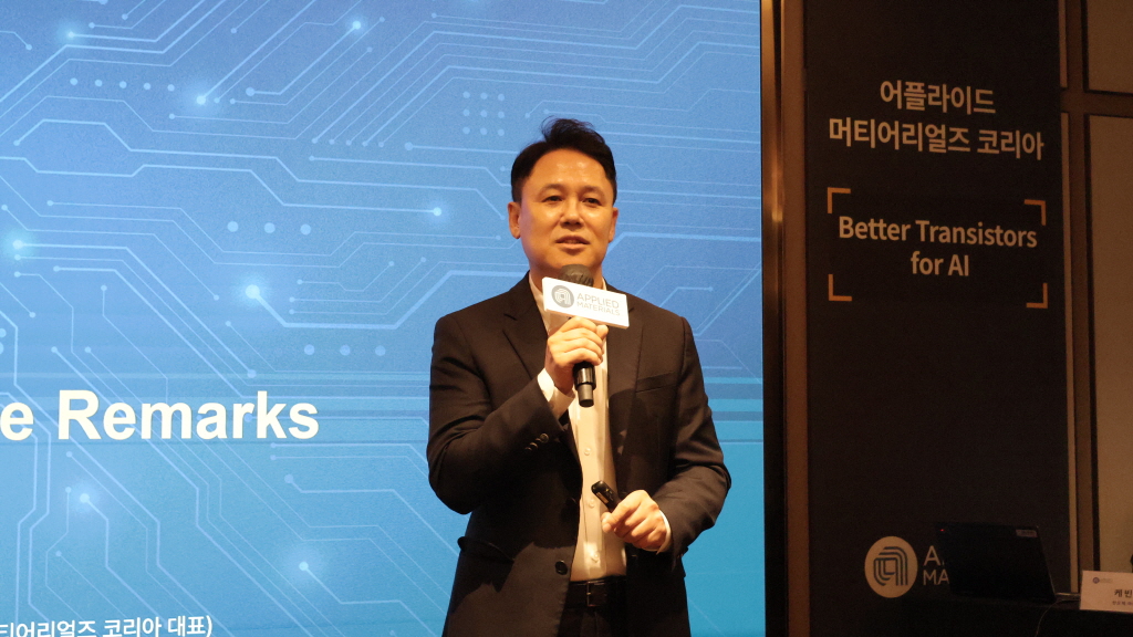
▲박광선 어플라이드 머티어리얼즈 코리아 대표이사가 환영사를 하고 있다.
Viva 라디칼 처리 시스템·Sym3 Z Magnum 식각 시스템·Spectral ALD 시스템

어플라이드 머티어리얼즈(Applied Materials)가 인공지능(AI) 확산에 따른 반도체 기술 패러다임 변화에 대응하기 위해 차세대 로직 공정용 신제품 3종을 공개했다.
어플라이드는 12일 조선 팰리스 서울 강남에서 미디어 간담회를 열고, AI 반도체의 성능과 에너지 효율을 동시에 끌어올릴 수 있는 핵심 공정 장비를 선보였다.
이날 행사는 박광선 어플라이드 머티어리얼즈 코리아 대표이사의 환영사로 시작됐다.
박광선 대표는 “AI 반도체 성능이 단일 칩의 한계에 직면한 상황에서, 로직·메모리·패키징을 아우르는 시스템 차원의 공동 최적화가 필수적”이라며 “어플라이드는 고객과의 협력을 통해 기술 개발 속도를 획기적으로 단축할 수 있는 생태계를 구축하고 있다”고 강조했다.
박광선 대표는 미국 실리콘밸리에 개소 예정인 ‘에픽 센터’와 한국 협업 거점인 ‘코리아 컬래버레이션 센터’를 통해 글로벌 반도체 협력을 강화하겠다는 계획도 밝혔다.
이어 케빈 모라스 어플라이드 머티어리얼즈 반도체 제품 마케팅 부사장은 AI 확산이 가져올 산업 구조 변화를 짚었다.
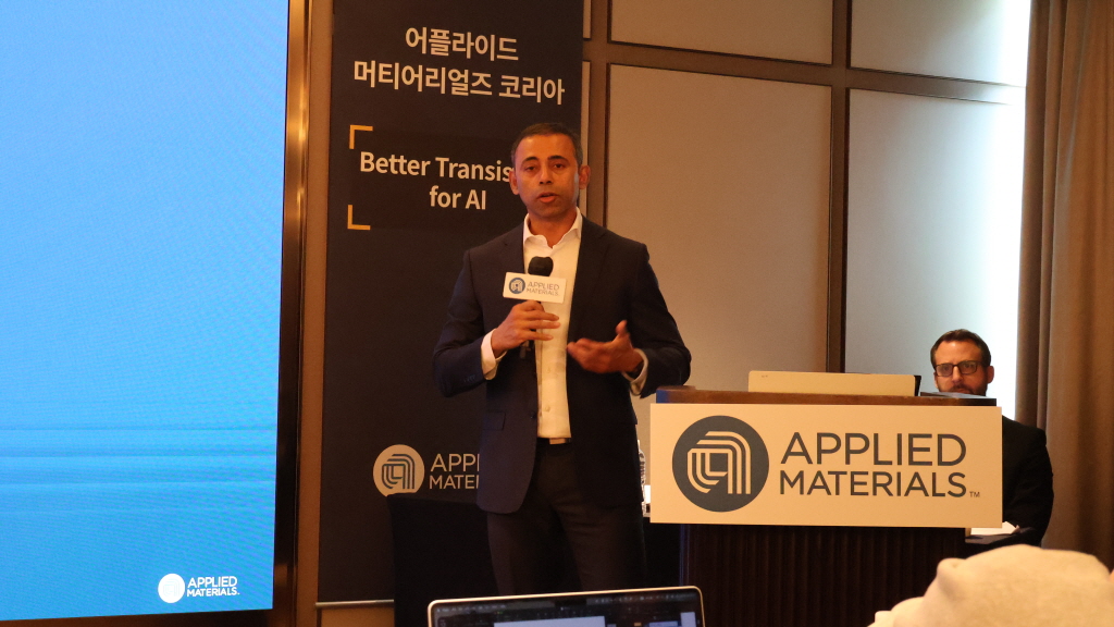
▲케빈 모라스(Kevin Moraes) 어플라이드 머티얼리얼즈 반도체 제품 마케팅 부사장이 업계 트렌드를 소개하고 있다.
케빈 모라스 부사장은 “AI는 클라우드 데이터센터를 넘어 자율주행, 로보틱스, 가정용 기기 등 모든 영역으로 확산되고 있다”며 “문제는 에너지”라고 지적했다.
AI 데이터센터의 전력 소비가 한국 연간 전력 사용량의 두 배에 달할 수 있다는 전망을 언급하며, 2040년까지 AI 스택 전반에서 1만 배 이상의 에너지 효율 개선이 필요하다고 강조했다.
이를 위해서는 소프트웨어부터 칩 설계, 제조 공정까지 전 영역의 혁신과 협업이 필수라는 설명이다.
이날 행사의 핵심은 마이클 추지크 어플라이드 머티어리얼즈 반도체 기술 부사장이 발표한 로직 공정용 신제품 3종이다.
.jpg)
▲마이클 추지크(Michael Chuzik) 어플라이드 머티얼리얼즈 반도체 기술 부사장이 신제품 3종을 발표하고 있다.
추지크 부사장은 “AI 혁명의 중심에는 GPU가 있으며, GPU 성능과 전력 효율은 트랜지스터 구조 혁신에 달려 있다”고 말했다.
특히 2나노미터 공정에서 본격화되는 GAA(Gate-All-Around) 구조는 성능 향상과 저전력 구현의 핵심이지만, 제조 난이도가 급격히 높아진다는 점을 강조했다.
첫 번째 신제품은 ‘비바(Viva) 라디컬 처리 시스템’이다. 이 장비는 GAA 나노시트 구조에서 실리콘 표면을 원자 수준으로 정밀하게 정제해, 전하 이동 시 발생하는 산란을 최소화한다.
이를 통해 캐리어 이동도를 높이고, 결과적으로 트랜지스터 성능과 에너지 효율을 동시에 개선할 수 있다.
추지크 부사장은 “표면의 미세한 거칠기와 오염을 제거하는 것이 3D 나노시트 성능의 출발점”이라고 설명했다.
두 번째는 ‘심(Sym) 3Z 매그넘 식각 장비’다.
이 장비는 3차원으로 적층된 나노시트 각각에 균일하게 접근할 수 있도록, 매우 수직적이고 매끄러운 콘택트 홀을 형성한다.
정밀한 이온 제어 기술을 통해 상·중·하단 나노시트 모두에 동일한 전기적 특성을 구현할 수 있어, 차세대 로직 소자의 신뢰성과 수율을 높이는 데 기여한다.
세 번째 신제품은 ‘스펙트라(Spectra) 몰리브덴 ALD 시스템’이다.
이 장비는 콘택트 홀 내부에 선택적으로 몰리브덴을 증착해 저저항 금속 연결을 구현한다.
고집적 GAA 구조에서 신호 손실을 최소화하고, 고성능·저전력 AI 칩 구현을 가능하게 하는 핵심 기술로 평가된다.
추지크 부사장은 “AI 시대의 반도체는 더 빠르고, 더 적은 에너지로 동작해야 한다”며 “이번에 공개한 세 가지 신제품은 3D 로직 소자의 복잡성을 극복하고, AI 확산을 지속 가능하게 만드는 중요한 기술적 전환점이 될 것”이라고 말했다.

Comments
Related news
Applied Materials forecasts $7.1 billion in sales in Q2 2025, maintaining strong performance amidst semiconductor market growth.
Global semiconductor and display materials engineering solutions company Applied Materials announced its fiscal year 2025 second quarter results. Global revenue for this quarter reached $7.1 billion, representing a 7% increase compared to the same period last year, reflecting strong performance sustained by continuous growth in the semiconductor market and technological innovation.
2025.05.16by 배종인 기자
.jpg)
Applied Materials' Q3 global sales reached $7.3 billion, up 8% year-over-year, achieving record sales.
Applied Materials, a leading materials engineering solutions provider for advanced semiconductors and displays worldwide, recorded record quarterly revenue of $7.3 billion in the third quarter of fiscal year 2025, which ended on July 27.
2025.08.18by 명세환 기자
.jpg)
Applied Materials Launches Environmental Protection Campaign to Mark World Cleanup Day
Applied Materials Korea (CEO Park Kwang-seon) is carrying out environmental cleanup activities with employees and their families around the Dongtan Sinricheon area on the occasion of World Cleanup Day, evolving into a company that engages with the local community beyond technological innovation.
2025.09.22by 명세환 기자
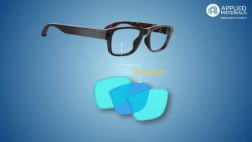
Applied Materials and GlobalFoundries Partner to Develop AI-Based Photonics
Applied Materials has entered into a strategic partnership with GlobalFoundries and will establish a state-of-the-art waveguide manufacturing facility in Singapore. This collaboration is aimed at accelerating technological innovation in AI-based photonics, and the two companies plan to jointly develop high-performance optical solutions for implementing next-generation digital experiences by combining their expertise in semiconductors and materials engineering.
2025.10.02by 명세환 기자
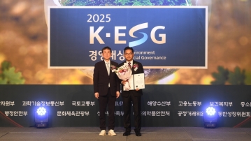
Applied Materials Recognizes Sustainability Through ESG
Applied Materials Korea (CEO Park Kwang-seon) received both the 'Grand Prize in ESG Division' and the 'Minister of Foreign Affairs Award' at the '2025 K-ESG Management Awards' ceremony, establishing itself as a model company for sustainable management.
2025.10.22by 명세환 기자











