


Kim Jae-young, Managing Director at Qualitas Semiconductor, “Anritsu ShockLine™ VNA 'MS46524B', the Standard for Ultra-High Speed Interconnect Reliability Chosen by Qualitas”
 Published2026.03.08 18:01
안리쓰 ShockLine™ VNA ‘MS46524B’”
PCB·패키지·테스트 칩 전반 차등 사전 검증 가능, IP 품질 신뢰성 제공
[편집자주]대한민국에 본사를 둔 퀄리타스 반도체(Qualitas Semiconductor Co., Ltd., 이하 ‘퀄리타스’)는 초고속 인터커넥트 기술 분야의 선도 기업으로, 차세대 AI, 자동차, 모바일 및 디스플레이 분야에 첨단 솔루션을 제공한다. 퀄리타스는 최첨단 반도체 공정 기술과 고성능 회로 설계 전문성을 바탕으로 높은 신뢰성과 실리콘 검증을 거친 IP 솔루션을 개발한다. 이러한 솔루션은 고객이 시스템 통합을 가속화하고, 신제품 개발 속도를 높이며, 혁신을 주도할 수 있도록 지원한다.
초고속 인터페이스 기술의 발전으로 PHY IP의 성능을 최대한 구현하기 위해서는 칩의 특성뿐만 아니라 PCB(인쇄회로기판)와 소켓을 포함한 전체 인터커넥트 채널의 전송 손실 및 전송/반사 특성까지 고려해야 한다. 나아가, 미래의 다양한 패키지 및 인터커넥트 구조를 수용할 수 있는 재현성이 높은 검증 환경을 구축하는 것이 필수적이다.
이러한 과제를 해결하기 위해 퀄리타스는 안리쓰 ShockLine™ 벡터 네트워크 분석기(VNA) MS46524B를 사용했다. 이를 통해 퀄리타스는 PHY IP를 포함한 시스템 전체의 신호 무결성을 검증할 수 있는 역량을 강화하여 고객에게 제공하는 솔루션의 품질과 신뢰성을 보장할 수 있게 되었다.
이에 본지는 퀄리타스 반도체의 광 인터커넥트 R&D 센터에서 활발히 활동 중인 김재영 상무이사를 인터뷰했다. 안리쓰의 테스트 솔루션이 퀄리타스의 초고속 인터커넥트 PHY IP 솔루션에 어떻게 활용되고 있는지, 그리고 어떤 성과를 거두었는지에 대해 질문했다. 본 기사에서는 차세대 반도체 인터페이스의 신뢰성 확보를 위한 첨단 검증 기술과 글로벌 시장 경쟁력 유지를 위한 품질 보증 시스템 구축 사례를 소개한다.
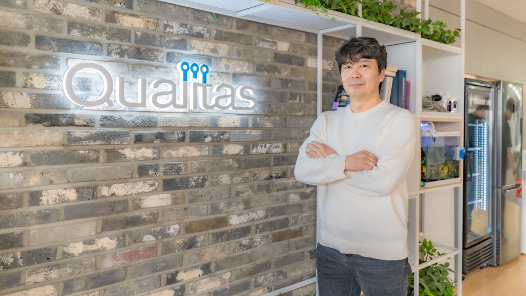
▲김재영 퀄리타스 반도체 상무이사

■ Qualitas의 사업과 강점에 대해 듣고 싶다
퀄리타스반도체는 초고속 인터커넥트를 위한 PHY IP 솔루션 개발 전문 기업으로, 고대역폭·고속 신호 전송 환경에서 필수적인 신호 무결성(Signal Integrity) 기술을 핵심 경쟁력으로 보유하고 있다. 당사는 SERDES PHY IP를 비롯해 PCI Express®(PCIe®) PHY IP, UCIe(Universal Chiplet Interconnect Express) 솔루션, 이더넷 PHY IP, MIPI 및 디스플레이 솔루션, SLVS-EC RX PHY IP, USB SuperSpeed+ PHY IP 등 폭넓고 고부가가치의 초고속 인터페이스 PHY IP 포트폴리오를 제공하고 있다.
퀄리타스반도체는 이러한 기술 경쟁력을 바탕으로 미국, 중국, 일본을 포함한 글로벌 주요 반도체 시장에서 선도적인 고객사들과 다수의 IP 공급 및 협력 계약을 체결해 왔으며, 다양한 응용 분야와 시스템 환경에서 검증된 실리콘 레퍼런스와 양산 경험을 축적해 왔다.
또한, 선단 공정 및 복잡한 시스템 요구사항에 최적화된 설계 역량을 통해 고객의 설계 복잡도와 통합 리스크를 최소화하고 개발 기간 단축 및 안정적인 양산을 지원한다. 이러한 기술력과 글로벌 고객 기반을 바탕으로 퀄리타스반도체는 AI, 데이터센터, 자동차, Chiplet 기반 시스템 등 차세대 반도체 인터페이스 시장에서 신뢰받는 핵심 기술 파트너로서 입지를 지속적으로 확대하고 있다.
■ 최근 초고속 인터커넥트 PHY IP 개발에서 신호 무결성 검증이 더욱 중요해진 이유는 무엇인지 궁금하다
최근 PCIe, UCIe, USB, 이더넷 등 주요 인터페이스 표준의 데이터 전송 속도가 지속적으로 향상되고 있다. 이에 따라 시스템 전송 용량과 응답성 향상에 대한 수요가 증가하고 있으며, 다양한 반도체 제품 또한 고성능 및 고밀도로 발전하고 있다. 이러한 환경에서는 개별 칩의 성능만으로는 실제 사용 환경에서 요구되는 품질과 신뢰성을 보장하기에 더 이상 충분하지 않다.
실제 시스템 환경에서는 칩 자체뿐만 아니라 PCB와 소켓을 포함한 전체 인터커넥트 채널이 고속 신호 전송에 큰 영향을 미친다. 전송선로를 따라 발생하는 손실, 반사, 누화는 신호 무결성 저하를 초래한다. 따라서 이러한 모든 요소를 고려한 포괄적이고 정확한 신호 무결성 검증이 필수적이다. 특히 속도가 증가함에 따라 인터커넥트 특성의 미세한 변화조차도 전체 시스템 안정성과 데이터 품질에 직접적인 영향을 미칠 수 있으므로, 그 어느 때보다 더욱 정밀한 검증 방법이 요구된다.
■ 퀄리타스는 이러한 기술적 과제를 해결하기 위해 어떤 계획을 추진하고 있는지 듣고 싶다
퀄리타스는 초고속 인터페이스 시장의 발전과 점점 더 정교해지는 고객 요구에 대응하여 기존의 시뮬레이션 기반 검증에서 실제 환경과 매우 유사한 사전 검증 시스템으로 전환하고 있다. 구체적으로, 패키지 및 PCB에 IP 칩을 구현한 후 차동 S-파라미터 및 시간 영역 반사 측정(TDR)과 같은 파라미터를 사용하여 신호 무결성을 정량적으로 검증하는 자체 개발 방법을 도입했다. 이 접근 방식을 통해 개발 초기 단계부터 시스템 수준의 신뢰성을 확보하고 고객에게 고품질의 실용적인 PHY IP를 제공할 수 있다.
■ 이러한 계획들의 배경과 기술적 문제에 대해 설명을 한다면
이러한 계획의 배경에는 기존 시뮬레이션만으로는 실제 구현 환경에서 발생하는 손실, 반사, 전송선로 간 누화와 같은 신호 무결성 특성을 완벽하게 재현할 수 없다는 한계가 있었다. 그 결과, 설계 주기를 단축하고 고객의 까다로운 신뢰성 요구 사항을 충족하는 데 제약이 있었다. 전 세계 고객들은 보다 정량적이고 재현 가능한 검증 데이터의 제출을 강력하게 요구하고 있다. 이러한 상황을 고려하여 신호 무결성 검증 역량을 강화하고, 향후 다양한 패키지 구조 및 차세대 인터페이스 기술에 적용할 수 있는 기반을 마련하는 것이 필요했다.
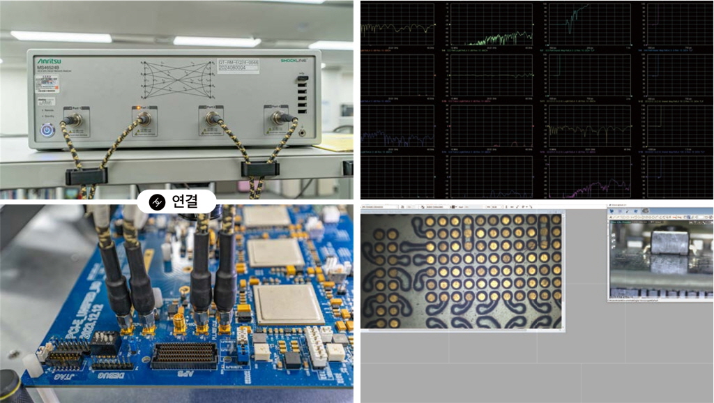
▲안리쓰 ShockLine™ VNA ‘MS46524B’와 측정화면
■ 안리츠 Shockline VNA MS46524B를 선택하게 된 결정적인 이유와 그 결과로 얻은 성과에 대해 듣고 싶다
VNA를 도입할 때 여러 시험 및 측정 장비 업체의 제품을 비교했다. 안리쓰의 ShockLine VNA MS46524B를 선택한 주요 이유는 고주파수 대역에서의 측정 안정성, 프로브와 동축 케이블이 혼합된 환경에 대한 유연한 적응성, 그리고 맞춤형 소프트웨어를 통한 워크플로우 최적화와 같은 다른 회사 제품에서는 찾아볼 수 없는 포괄적인 강점 때문이다.
MS46524B는 4포트 구성 덕분에 안정적인 측정이 가능하다. 또한, 안리쓰 고유의 확장형 K-타입 커넥터 기술을 활용하여 프로브 기반 측정에서도 안정적인 데이터 수집이 가능하다. 뿐만 아니라, 10피코초 미만의 고해상도 TDR 측정을 지원하여 소형 패키지 및 미세한 임피던스 변화까지 매우 정밀하게 검증할 수 있다. 이러한 특징 덕분에 VNA 도입 후 PCB와 테스트 칩을 단일 플랫폼에서 효율적으로 검증할 수 있는 환경을 구축할 수 있었다. 나아가 검증 주기를 단축하고 글로벌 고객에게 품질 평가 보고서를 제출하는 데 걸리는 시간을 크게 줄였다. 결과적으로 퀄리타스의 고객은 더욱 안정적인 IP를 더 짧은 시간 안에 구현할 수 있게 되어 제품 개발 위험을 줄이고 시장 출시 시간을 단축할 수 있다.
주파수 영역과 시간 영역 모두에서 상호 연결 특성을 검증하는 대표적인 방법으로는 차동 S-파라미터 측정과 차동 TDR 측정이 있다. 차동 S-파라미터 측정은 채널 삽입 손실, 반사 특성, 차동 전송 특성을 정량적으로 평가할 수 있어 전체 신호 전송 성능을 수치적으로 파악할 수 있다. 반면, 차동 TDR 측정은 패키지 및 PCB 내부의 임피던스 불연속성뿐만 아니라 미묘한 구조적 문제까지 시간 영역에서 직관적으로 포착할 수 있다는 장점이 있다. 이 두 가지 방법을 병행하여 활용하면 사양 충족 여부 확인은 물론, 문제 발생 시 다각적인 관점에서 근본 원인을 분석할 수 있다. 결과적으로 PHY IP 설계 단계에서 고품질 피드백을 얻을 수 있으며, 이는 설계, 검증, 개선의 선순환 구조를 구축하는 데 매우 중요한 역할을 한다.
■ 초고속 인터커넥트 검증 환경을 구축하면서 겪었던 문제점과 해결 방법에 대해 듣고 싶다
프로브 기반 비동축(프로브-동축, 프로브-프로브) 검증 환경 구축 시 주요 과제는 ‘기준면 설정’과 측정 재현성 확보였다. 특히 볼패드형 패키지나 정밀 PCB 패턴을 검증할 때 프로브 접촉 상태나 위치 차이로 인해 검증 결과에 변동이 발생하여 정밀한 신호 무결성 검증이 어려웠다. 이러한 문제를 해결하기 위해 ShockLine VNA MS46524B를 활용하여 프로브-동축 및 프로브-프로브 측정을 모두 지원하는 4포트 테스트 환경을 구축했다. 또한, Type-E 네트워크 추출 기술과 디임베딩 기법을 적극적으로 적용하고 프로브 스테이션 연결 조건 및 검증 절차를 표준화했다. 나아가, 안리츠의 맞춤형 소프트웨어를 통해 프로세스를 자동화함으로써 검증의 안정성과 재현성을 크게 향상시켰다.
■ 프로브 기반 검증에서 해결해야 할 문제점이 있는지 궁금하다
프로브 기반 측정은 고속 인터페이스 검증에 필수적인 방법이지만, 실제 시스템 환경과의 차이를 최소화하는 것이 중요하다. 이러한 이유로 퀄리타스에서는 패드 레벨 측정뿐만 아니라 실제 패키지 구조와 PCB 레이아웃을 충실하게 재현한 평가 보드(EVB)를 설계하고 이를 사용하여 검증을 수행한다. 또한 프로브-동축 및 프로브-프로브 환경 모두에서 차동 S-파라미터 측정과 차동 TDR 측정을 병렬로 수행하고 각 측정 방법의 특성을 정량적으로 비교 분석한다. 그 결과, 실제 사용 환경에 가까운 신호 무결성 특성을 사전에 평가할 수 있어 고객 시스템의 예측 정확도와 IP 신뢰성 향상에 기여한다.
■ 초고속 인터커넥트의 신호 무결성 검증 과정에서 디임베딩 기술은 매우 중요하게 여겨진다. Qualitas에서는 디임베딩 기술을 어떻게 활용하고 있으며, 그 효과는 무엇인지 설명한다면
초고속 인터커넥트의 경우, 측정 시스템에 포함된 프로브, 케이블, 어댑터 등의 외부 구성 요소가 측정 결과에 영향을 미치므로 디임베딩 기술을 이용한 보정이 필수적이다. 퀄리타스에서는 MS46524B를 사용한 4포트 측정 환경에서 프로브와 어댑터의 S-파라미터를 사전에 추출한다. 그런 다음 디임베딩 기술을 적용하여 DUT(테스트 대상 장치)의 고유 특성을 정확하게 검증할 수 있다.
이 방법을 통해 삽입 손실 및 임피던스 특성과 관련된 측정 오차를 크게 줄일 수 있으며, 손실이 큰 채널이나 마이크로 패키지 구조에서도 신뢰할 수 있는 신호 무결성 검증이 가능하다. 또한, 검증 결과는 PHY IP 설계 단계에서 구체적인 피드백으로 활용되어 설계를 최적화하고 품질을 향상시키는 데 도움이 된다.
■ 검증 환경 구축이 퀄리타스의 지적 재산 품질 및 향후 기술 개발 전략에 어떤 영향을 미쳤는지 궁금하다
안리쓰의 ShockLine VNA MS46524B 도입으로 IP 벤더 레벨에서 패키지 및 인터커넥트 성능 사전 검증 시스템이 구축됐다. 이를 통해 고주파 영역에서 효율적인 반복 측정이 가능해졌으며, 안리쓰의 맞춤형 소프트웨어는 검증의 재현성과 작업 효율성을 크게 향상시켰다. 결과적으로 PCB, 패키지, 테스트 칩 전반에 걸친 차등 사전 검증이 가능해져 최종 사용자에게 더욱 높은 IP 품질 신뢰성을 제공할 수 있게 되었다. 앞으로 이러한 검증 환경을 기반으로 다양한 패키지 구조 및 차세대 고속 인터페이스 기술로 확장하여 퀄리타스의 신호 무결성 경쟁력을 더욱 강화할 계획이다.
■ 퀄리타스는 차세대 초고속 인터페이스 지원을 준비하면서 향후 신호 무결성 검증 환경을 어떻게 더욱 발전시킬 계획인지 알고 싶다
미래 인터페이스 기술의 발전과 함께 패키지 구조의 다양화, 칩렛 기반 아키텍처의 확산, 그리고 데이터 전송 속도의 지속적인 가속화로 인해 신호 무결성 검증이 더욱 어려워질 것으로 예상된다. 퀄리타스는 고주파 대역에서의 차동 측정 기능을 강화할 뿐만 아니라 더욱 복잡한 패키지 및 인터커넥트 구조를 수용할 수 있는 재현성이 높은 검증 환경 구축에 주력하고 있다. ShockLine VNA MS46524B와 통합된 프로브 기반 측정 소프트웨어를 중심으로 하는 신호 무결성 검증 플랫폼을 지속적으로 확장하여 UCIe 및 PCIe Gen6와 같은 차세대 표준에 대한 지원을 더욱 강화하고 있다. 또한, 업계 표준화 활동 및 타 기업과의 공동 연구에 적극적으로 참여함으로써 반도체 인터페이스 분야의 전반적인 품질 향상에 기여하고자 한다.
■ 초고속 인터커넥트 개발 업체가 글로벌 시장에서 경쟁력을 더욱 강화하기 위해 필요한 요소는 무엇인지 의견을 듣고 싶다
초고속 인터커넥트 개발 업체에게 가장 중요한 것은 사양을 충족하는 IP를 제공하는 것 뿐만 아니라 고객의 실제 시스템 환경에서 높은 신뢰성을 입증하는 것이다. 글로벌 고객은 고급 IP 성능 검증 뿐만 아니라 패키지, PCB 및 소켓을 포함한 전체 인터커넥트에 대한 신호 무결성 검증 결과 제출을 요구할 수도 있다.
퀄리타스는 IP 개발 초기 단계부터 실제 패키지 및 PCB 환경에서 사전 검증 시스템을 구축하여 차동 S-파라미터 및 TDR과 같은 정량적 데이터를 활용해 IP 품질을 객관적으로 평가한다. 또한 ShockLine VNA MS46524B와 같은 고신뢰성 테스트 솔루션을 활용하여 글로벌 고객의 요구 사항을 충족하는 검증 데이터를 선제적으로 제공할 수 있는 체계를 구축했다. 이는 퀄리타스의 기술적 신뢰성과 수주 경쟁력을 확보하는 주요 차별화 요소가 됐다.
■ 안리쓰와의 협업에서 특히 인상적이었던 측면이나 계획에 대해 이야기 한다면
이번 협력에서 안리쓰는 VNA 장비 공급뿐 아니라 당사의 검증 환경과 워크플로우를 깊이 이해하고, 당사의 요구에 맞춘 기술 지원을 제공해 주었다. 특히, 고주파 측정 및 복잡한 절차를 효율적으로 실행할 수 있는 맞춤형 소프트웨어를 공동 개발하여 작업 효율성과 측정 신뢰성을 크게 향상시켰다. 그 결과, VNA 장비 도입 이후에도 기술 개발 및 검증 환경을 지속적으로 확장할 수 있는 신뢰 관계를 구축했으며, 차세대 인터페이스 검증 분야의 기술 파트너로서 장기적인 협력 기반을 마련했다.
※ PCI-SIG®, PCIe® 및 PCI Express®는 PCI-SIG의 등록 상표다.
※ 위 인터뷰와 관련한 케이스 스터디 PDF는 아래에서 다운로드 받을 수 있다.

Comments
Related news
Park Se-ho, Director of RAPA IoT Technology Support Center, “Providing a test environment for 5G-A and 6G next-generation communication fields”
[Editor's Note] As the next-generation communications era begins, there is a need to establish infrastructure capable of testing and validating 5G-Advanced/6G technologies. Accordingly, the Korea Radio Promotion Association and Anritsu have begun collaborative efforts to build a verification environment for next-generation communications technologies. Anritsu has agreed with the Korea Radio Promotion Association (hereinafter RAPA) to collaborate on technology verification for the next-generation communications standards 5G-A/6G. To hear about the collaborative achievements of RAPA and Anritsu in promoting next-generation communications technology and industry development, we met with Park Se-ho, Director of RAPA's IoT Technology Support Center, and Lim Hyun-muk, Deputy Manager of Technical Support at Anritsu Corporation, to discuss cooperation with Anritsu.
2024.10.18by 권신혁 기자
Anritsu to present latest 6G connectivity line at MWC 2025
Anritsu Corporation will showcase a variety of solutions at the Mobile World Congress (MWC) 2025 booth 5D41 in Barcelona, including AI-based testing tools, virtualization solutions for accelerating UE protocol development, digital twin simulation environments for C-V2X, and NTN mobility device testing.
2025.02.05by 배종인 기자
On-device AI improves smartphone communication quality
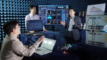
SK Telecom (CEO Yoo Young-sang) has successfully developed and demonstrated a technology that increases the number of antennas embedded in smartphones to enhance communication performance, in collaboration with Professor Hong Won-bin's team from the Department of Electrical Engineering at POSTECH (Pohang University of Science and Technology). In this demonstration conducted in a laboratory environment, SKT confirmed that data transmission speed was meaningfully improved under identical conditions as existing smartphones by utilizing measurement equipment from Anritsu, a global telecommunications measurement equipment company.
2025.02.06by 배종인 기자
Anritsu Announces Wi-Fi 7 OTA Test Solution Supporting High-Speed Communications
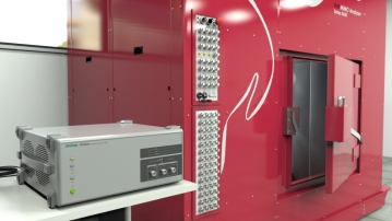
EMITE and Anritsu announced an enhanced OTA (Over-the-Air) measurement solution on the 20th that conforms to the 2x2 MIMO specifications of the latest wireless LAN standard IEEE 802.11be.
2025.02.21by 명세환 기자
.jpg)
Anritsu to Take Responsibility for Compound Semiconductor MPW Process Reliability Testing
Anritsu, a leading global test and measurement equipment provider, has signed an MOU with the Compound Semiconductor Research Center (CSRC) at Mokpo National University (President Song Ha-chul), taking responsibility for reliability testing in the final stage of Korea's first compound semiconductor MPW (Multi-Project Wafer) process. To support this initiative, Anritsu is providing high-performance measurement equipment valued at approximately 1.5 billion won to Mokpo National University's Compound Semiconductor Research Center.
2025.02.27by 권신혁 기자











