


Korea University and DGIST Innovate Laser-Based 3D Stacked DRAM
 Published2026.04.17 15:57
.jpg)
▲ From left: Professor Yoo Hyun-yong of Korea University, PhD candidate Park Jong-yoon of Korea University, Professor Kwon Hyuk-jun of DGIST, PhD candidate Jung Hee-jae of DGIST [Photo credit: Korea University, DGIST]
Domestic researchers have achieved a result that significantly exceeds the performance limits of 3D stacked DRAM by combining a laser crystallization process and a heterogeneous channel design.
Professor Hyun-Yong Yoo of Korea University and Professor Hyuk-Joon Kwon's team at DGIST announced on the 17th that they have implemented a complementary gain cell (CGC) structure by vertically stacking a silicon layer (p-Si) and an oxide semiconductor (n-IGZO) made by pattern-based seedless laser crystallization (PSLC) for the first time in the world, thereby simultaneously boosting the speed and sensing capabilities of 2T0C DRAM.
The research team secured a grain size of 32.3 µm through a laser process, and as a result, the hole mobility reached 265 cm²/Vs.
In addition, by utilizing the capacitive coupling between devices, which was previously pointed out as a problem, in reverse to obtain a voltage amplification effect, the sensing margin was improved to a level of tens to hundreds of times compared to the previous one.
Simulation and measurement results showed that the read delay was about 11.8ns, which is about 7.6 times faster than an IGZO-only cell (about 90.1ns), and reliability was also verified by securing a retention time of more than 1,000 seconds.
Since all processes are carried out at 400℃ or below, memory layers can be stacked without damaging the underlying logic, allowing for monolithic 3D (M3D) It is also noteworthy that it is suitable for integration.
The research team expected this technology to be a significant turning point in the commercialization of high-density, high-performance memory and memory solutions for AI chips.
This research was accepted to the VLSI Technology Symposium 2026 and was conducted with support from the Ministry of Science and ICT and the National Research Foundation of Korea.

Comments
Related news
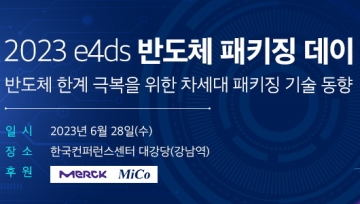
Overcoming semiconductor limitations is now packaging
Intel, Nexpak, Applied Materials, Hyundai Securities, Next-Generation Intelligent Semiconductor Business Division, and Hanyang University will host the "2023 e4ds Semiconductor Packaging Day," a specialized seminar on semiconductor packaging, on Wednesday, June 28 at the Grand Auditorium of Korea Conference Center.
2023.06.07by 명세환 기자
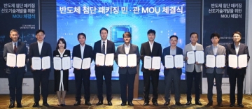
Semiconductor Advanced Packaging, Public-Private Partnership
The Ministry of Trade, Industry and Energy, Samsung Electronics, SK Hynix, LG Chem, Hana Micron, Protec, Sapion Korea, Simtec, the Next-Generation Intelligent Semiconductor Business Division, the Korea Semiconductor Industry Association, the Korea Institute of Industrial Technology Evaluation and Planning, and other companies in the materials, parts and equipment (MPM) sector, semiconductor advanced packaging specialists (OSAT), and fabless enterprises concluded an agreement on cooperation for semiconductor advanced packaging technology development.
2023.08.29by 배종인 기자
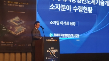
“Next-generation intelligent semiconductor, targeting 1 teraflops of computing efficiency by 2029”
Lee Seok-hee, team leader of the Device Team at the Next-Generation Intelligent Semiconductor Business Division, presented "2025 Next-Generation Intelligent Semiconductor Technology Development Project Device Sector Implementation Status" at the '2025 Neuromorphic Semiconductor Workshop' held at L Tower on the 19th. He stated, "Researchers aim to complete next-generation semiconductor technology with 1 teraflops of computational performance by implementing a prototype by 2029," and added, "To achieve this, foundational technology acquisition, core design, and platform construction will be carried out."
2025.05.26by 배종인 기자
.jpg)
Next-Generation Intelligent Semiconductor Technology Development Project Achieves 1,426 Patents and Creates 1,628 Jobs Over 5 Years
The Ministry of Science and Technology (Minister Bae Gyeong-hun) and the Ministry of Trade, Industry and Energy (Minister Kim Jeong-gwan) jointly hosted the "2025 Next-Generation Intelligent Semiconductor Technology Development Project Integrated Technology Exchange Conference" in Jeju for two days from October 27 to 28. The event was organized by the Next-Generation Intelligent Semiconductor Business Division (Director Kim Hyeong-jun), bringing together approximately 550 researchers from industry, academia, and research institutions representing Korea's semiconductor sector to share research achievements and technology trends while strengthening collaborative networks.
2025.10.27by 명세환 기자
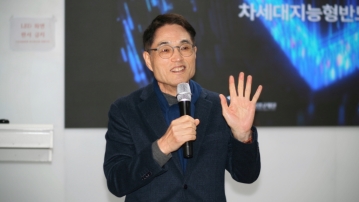
Securing Next-Generation Optical Packaging Technology Depends on Interest and Talent Development
The Next-Generation Intelligent Semiconductor Business Division (Director Kim Hyung-jun) and Seoul National University of Science and Technology hosted the "2025 2nd Advanced Optical Packaging Technology Seminar" on the 17th at Seoul Tech's Eo-ui Hall, where they discussed the latest technology trends in the optical packaging field, cultivation of specialized personnel to meet industrial demands, and focused discussions on the possibilities and challenges of glass substrates as next-generation packaging materials, presenting insights for the advancement of Korea's optical packaging technology.
2025.12.19by 배종인 기자











