◇ 15.6 Trillion Won Investment in Pyeongtaek, Gyeonggi Province, Construction of One Advanced Semiconductor Line
- Largest investment in history for a single semiconductor production line
- Economic ripple effects expected to include '41 trillion won in production inducement' and '150,000 jobs inducement'
◇ Birth of a state-of-the-art semiconductor cluster connecting Giheung, Hwaseong, and Pyeongtaek
- Strengthening leadership in next-generation semiconductor markets such as mobile, server, and IoT
- Construction of state-of-the-art, eco-friendly semiconductor complex to begin full-scale operation in the first half of 2017
◇ Investment brought forward by more than a year due to tailored support for revitalizing the corporate economy, such as deregulation under the government's "Three-Year Plan for Economic Innovation"
- Government actively supports early supply of electricity and industrial water, and simplification of licensing procedures
- Synergy effects expected between promising future industries such as semiconductors and smart convergence products
◇ Vice Chairman Kwon Oh-hyun: "Pyeongtaek Complex Will Play a Major Role in Realizing the Future Creative Economy"
- Repaying the government's active support for early investment and the public's encouragement
- Contributing to the development of the national economy and local communities through research and development and investment
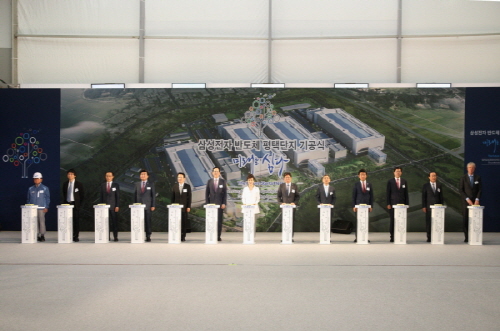
Samsung Electronics has commenced construction of the world's largest semiconductor production line in Pyeongtaek, Gyeonggi Province, ushering in the full-scale Pyeongtaek semiconductor era. On the 7th, Samsung Electronics [started construction] at the Godeok International in Pyeongtaek, Gyeonggi ProvinceSamsung Electronics held a groundbreaking ceremony for the Pyeongtaek Semiconductor Complex at the Hwaje Planning District Industrial Complex and commenced full-scale line construction.
The event, held under the slogan "Planting the Future," was attended by approximately 600 people, including President Park Geun-hye, Vice Chairman Lee Jae-yong, Minister of Trade, Industry and Energy Yoon Sang-jik, Gyeonggi Province Governor Nam Kyung-pil, Pyeongtaek Mayor Gong Jae-kwang, Samsung Electronics CEO Kwon Oh-hyun, and clients. The 'Samsung Electronics Pyeongtaek Semiconductor Complex' has a total site area of 2.89 million square meters (875,000 pyeong, equivalent to the size of about 400 soccer fields), a scale comparable to the combined area of the Giheung and Hwaseong complexes (910,000 pyeong), which are currently the largest semiconductor production complexes in Korea.
Samsung Electronics plans to build the largest semiconductor production line in its history on this site and execute a total investment of 15.6 trillion won in the first phase by 2017. This represents the largest investment in a single semiconductor production line in history.
This investment is expected to generate economic ripple effects such as 41 trillion won in production and the creation of 150,000 jobs, and is also expected to contribute significantly to revitalizing the national economy through the development of upstream and downstream industries such as materials and equipment.
※ Source: Bank of Korea Input-Output Table, based on production/employment inducement coefficients
The investment for the 'Samsung Electronics Pyeongtaek Semiconductor Complex' was decided more than a year ahead of schedule in accordance with the government's 'regional economic revitalization' policies, such as deregulation, which are being promoted as part of the 'Three-Year Economic Innovation Plan.'
In particular, the government has devised a plan to supply electricity, a core infrastructure of the semiconductor complex, early by the end of 2016, and has been actively supporting the Pyeongtaek Semiconductor Complex to begin operations early by ensuring a stable supply of industrial water and simplifying licensing procedures. Accordingly, Samsung Electronics plans to establish a close cooperative system with the government and local authorities in conjunction with the "Manufacturing Innovation 3.0 Strategy," which the government has been promoting since March of this year to revitalize the manufacturing sector. This initiative aims to ensure that the semiconductor industry serves as a core foundation for creating "representative new industries of the creative economy" and generates synergy with promising future industries. The newly established Pyeongtaek semiconductor line will be constructed as an eco-friendly line incorporating cutting-edge technology and is scheduled to begin full-scale operation in the first half of 2017.
In addition, the Pyeongtaek semiconductor line produces the latest semiconductor products, and recent demand It is expected to play a pivotal role in further strengthening leadership in the rapidly growing mobile and server markets and securing a leading position in the next-generation IoT (Internet of Things) market.
Samsung Electronics’ semiconductor business, which celebrated its 40th anniversary last December, has continuously developed in accordance with the government’s active policy to foster advanced industries, and currently maintains the number one position in the memory semiconductor market for 22 consecutive years.
In addition, as the system semiconductor sector is also facing an opportunity for a new leap forward, Samsung Electronics declared at the groundbreaking ceremony that the 'Pyeongtaek Semiconductor Complex' will be a new challenge for the next 40 years of semiconductor history.
In his welcoming remarks, Samsung Electronics CEO Kwon Oh-hyun stated, "Samsung Electronics' semiconductor business, which started in a technological wasteland, is preparing to take another leap forward for the future of South Korea," adding, "I hope the Pyeongtaek Semiconductor Complex will play a significant role in realizing the creative economy of the future." CEO Kwon also expressed his gratitude, saying, "Thanks to the active support from the government and local authorities, we were able to break ground on the Pyeongtaek Semiconductor Complex without any setbacks," and added, "To become the world's best semiconductor company, we will contribute to the development of the national economy and local communities through continuous research and development and investment, and repay the support of the people."
With the development of the Pyeongtaek Semiconductor Complex, various partner companies and clients are expected to move into the surrounding areas, and the world's largest state-of-the-art semiconductor cluster connecting Giheung, Hwaseong, and Pyeongtaek is projected to be formed.
Furthermore, the Pyeongtaek Semiconductor Complex is home to Samsung Electronics' semiconductor production facilities and IT R&D centers in Giheung and HwaIt is also expected to play a key role in establishing a large-scale IT valley connecting the Seoul metropolitan area and the Chungcheong region, serving as the central axis for Seongnam, Suwon, and the Cheonan-Asan region, where the display production complex is located.




 Published2015.05.12 12:59