


ACM Ships First SiCN Deposition Equipment… Expanding Support for Advanced BEOL and Packaging Processes
 Published2026.05.20 13:27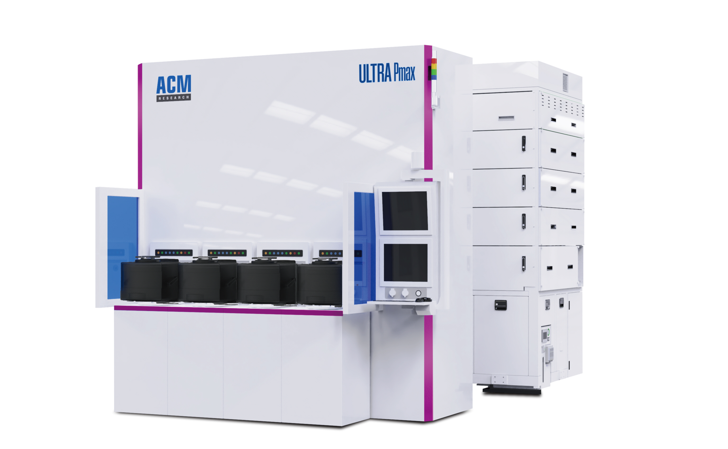
Application of a 3-station rotary PECVD structure enhances thin film uniformity and plasma control.
ACM announced on May 20 that it shipped its first PECVD SiCN system to a major semiconductor manufacturer. This equipment is a new addition to the Saturn series of ACM's planetary product family and is scheduled to enter field verification procedures after meeting the customer's process specifications at the Lingang Research Institute.
SiCN thin films are utilized in advanced wiring processes for copper oxidation inhibition, copper diffusion barriers, and etch stop layers. As logic semiconductors become miniaturized and wiring structures become more complex, there is an increasing demand for particle control, plasma stability, and interface layer control.
The scope of SiCN application is also expanding in advanced packaging. In next-generation integration processes such as wafer-level bonding, SiCN plays a role in enhancing integration reliability and suppressing metal ion diffusion based on its adhesion, bonding energy, and dense thin film characteristics.
ACM has applied a rotary deposition structure to this equipment, dividing the process into three stations within a single reaction chamber. Each station is designed to sequentially deposit a portion of the total film thickness to control gas flow, interface layer formation, and film uniformity across the entire wafer surface.
In addition, 'One Station, One RF' control technology was applied, featuring a dedicated RF system for each station. This allows for independent adjustment of plasma conditions for each station, focusing on enhancing process stability and consistency between stations.
The system supports the PECVD SiCN process for advanced BEOL processes of 55 nanometers or less. It is configured for 300mm wafer processes and features a maximum process temperature of 400 degrees, four load ports, and three process chambers to enhance wafer transfer efficiency and process operational flexibility.

Comments
Related news
.jpg)
ACM Research Sells Ultra C Equipment for SiC Cleaning
ACM Research, Inc., a specialist in wafer processing solutions for semiconductor and advanced wafer-level packaging (WLP) applications, has entered the power semiconductor market by securing its first purchase order for Ultra C equipment for SiC substrate cleaning.
2023.04.21by 배종인 기자
ACM Research Launches ULTRA C v Vacuum Cleaning Equipment
ACM Research, a specialized company providing wafer processing solutions for semiconductor and advanced wafer level packaging (WLP) applications, has announced a new vacuum cleaning solution that meets the new cleaning requirements of advanced 3D packages.
2023.09.27by 배종인 기자
ACM Research Enters Fan-Out Panel-Level Advanced Packaging Market
ACM Research, Inc., a specialist in wafer processing solutions for semiconductor and advanced wafer-level packaging (WLP) applications, has achieved economical and efficient advanced semiconductor packaging by enhancing cleaning efficiency through the utilization of vacuum technology and IPA drying technology.
2024.08.07by 배종인 기자
.jpg)
ACM Expands Fan-Out Panel-Level Packaging Portfolio
ACM Research, a leading provider of wafer processing solutions for semiconductor and advanced wafer-level packaging (WLP) applications, has launched the Ultra C bev-p panel bevel etching equipment for fan-out panel-level packaging (FOPLP) applications, enhancing process efficiency and reliability in copper-related applications while supporting high-precision characteristics on large panels.
2024.09.13by 배종인 기자

ACM, ALD process qualified for 300mm semiconductor mass production
ACM Research, Inc. has received process qualification certification from customers for its 300mm atomic layer deposition (ALD) furnace equipment for semiconductor mass production, and is now launching full-scale efforts to supply high-quality ultra-thin film deposition equipment and expand its customer base.
2024.12.12by 배종인 기자











