


UNIST Develops Charging Technology for Implantable Medical Devices to Reduce Battery Replacement Burden
 Published2026.05.27 13:20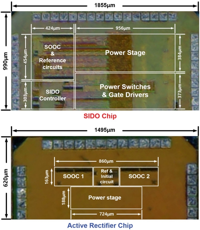
Switching power paths based on load conditions alleviates the burden of overheating and battery replacement
Ulsan National Institute of Science and Technology (UNIST) announced on the 27th that a research team led by Professor Young-Jae Byun of the Department of Electrical and Electronic Engineering has developed wireless power transmission technology that adjusts the power delivery structure in accordance with changes in power consumption of implantable medical devices.
This technology is characterized by a method of changing power delivery conditions based on the internal circuit characteristics of the device, which complements the limitations of existing fixed charging structures.
Implantable medical devices contain both high-load circuits requiring high current, such as nerve stimulation, and low-current based circuits, such as data processing. As load conditions change, optimal power delivery conditions also change; however, existing wireless charging methods fixed this to a single state, which resulted in power loss.
To solve this problem, the research team distinguished load conditions and applied a dedicated matching network tailored to each. Power transfer efficiency was enhanced by utilizing internal electronic switches to connect to the appropriate circuit depending on high or low load conditions.
The matching circuit is a circuit that regulates the efficient flow of power transmitted from an external transmitting coil into the medical device through a receiving coil, and is described as a key element of the power transmission process.
The research team improved not only power transmission but also the efficiency of the rectification process that converts alternating current (AC) to direct current (DC). Since the power delivered from the outside is in the form of alternating current, it must be converted to direct current to be used in medical devices.
The research team stated that a method for controlling switch operation timing was applied during this process, reducing losses occurring in the conversion phase.
Experimental results showed that the power transfer efficiency varied by condition: △low load (3mA) condition: link efficiency 94.4% △high load (30mA) condition: link efficiency 92.7% △rectifier conversion efficiency: maximum 94.5% △input voltage range of 2.5–5.0V: efficiency maintained at 92.3% or higher.
This figure was presented as a result demonstrating that stable power delivery is possible even with load changes and fluctuations in input conditions.
The research team explained that this technology could be used to extend the battery life of implantable medical devices used for extended periods, such as pacemakers and nerve stimulators. Accordingly, it is expected to contribute to alleviating the burden of periodic battery replacement surgeries.
In addition, the possibility was also presented that the same technology could be expanded into the field of low-power electronic devices, such as wearable devices and ultra-small Internet of Things (IoT) devices.
Meanwhile, this research was conducted with support from the Ministry of Science and ICT and the Institute of Information and Communication Technology Planning and Evaluation (IITP), and the results were published online on April 29 in the semiconductor circuit and systems journal 'IEEE Transactions on Very Large Scale Integration Systems'.

Comments
Related news
IBS, UNIST, and POSTECH Improve Room-Temperature Luminescence Performance of 2D Semiconductor Quantum Light Sources
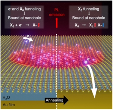
A joint research team from the Institute for Basic Science (IBS), UNIST, and POSTECH has improved the room-temperature luminescence performance of 2D semiconductor-based quantum light sources. The research team confined excitons, which easily diffuse at room temperature, within nanohole structures and reduced excess charges through heat treatment to improve light emission conditions. As a result, exciton confinement efficiency reached approximately 98%, and luminescence efficiency increased by approximately 130 times compared to previous results. The research results were published in the international journal Science Advances on March 13. This achievement demonstrates the potential to lead to research on photonic quantum devices with reduced cryogenic dependence and room-temperature single-photon light sources.
2026.04.14by 배종인 기자
KIMS and UNIST Develop Electrochemical System for Simultaneous Production of Hydrogen and Formate Using Waste Glycerol
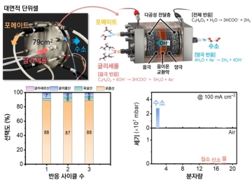
A joint research team from the Korea Institute of Materials Science and UNIST has developed an electrochemical system that produces hydrogen and formate simultaneously by utilizing glycerol, a biodiesel byproduct. The research team implemented an anion exchange membrane electrolysis system that applies glycerol oxidation reaction instead of the conventional oxygen evolution reaction in water electrolysis. Using a copper-cobalt-based non-precious metal catalyst, the team achieved 110 mA/cm² at 1.31 V, with formate selectivity of approximately 96%, and confirmed stable operation even in a large-area cell of 79 cm². The related research was published in the international academic journal Joule on March 18, 2026.
2026.04.14by 배종인 기자
UNIST Develops Smart Contact Lenses That Control Robotic Arms with Eye Movements
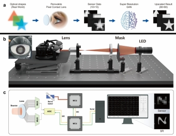
A research team led by Professor Jeong Im-du from the Department of Mechanical Engineering at UNIST has developed a smart contact lens that enables control of a robotic arm through eye movement alone. The lens surface features 100 optical sensors directly implemented on it that read gaze changes, and AI restores these into high-resolution information and converts it into control signals. The research results were published in Advanced Functional Materials in March 2026, and in eye model experiments, the system recognized nine-directional gaze gestures with 99.3% accuracy.
2026.04.15by 배종인 기자
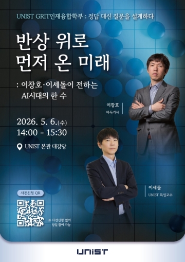
Lee Chang-ho and Lee Se-dol Discuss Human Capabilities in the AI Era at UNIST
UNIST will host an open talk concert on May 6 featuring Lee Chang-ho, a Go master, and Lee Se-dol, UNIST Distinguished Professor. The event will be held under the theme of human judgment, creativity, and perseverance in the AI era, and will serve as an occasion to introduce the educational direction of the newly established GRIT School of Talent Convergence.
2026.04.29by 명세환 기자
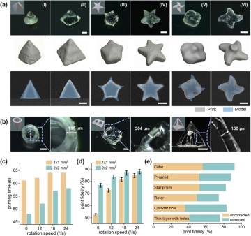
UNIST Develops 60-Second Micro 3D Printing Technology
A research team led by Professor Jung Im-du at ULSAN National Institute of Science and Technology (UNIST) has developed a droplet-based volumetric additive manufacturing technology that cures and dispenses structures within droplets in a single step. The research results were published in Advanced Functional Materials on March 21st, and the research team presented experimental results demonstrating continuous fabrication of different microstructures at approximately 60-second intervals.
2026.04.29by 명세환 기자











