


Samsung Electronics unveils zHBM and V10 BV-NAND mockups at FMS 2026
 Published2026.08.05 08:44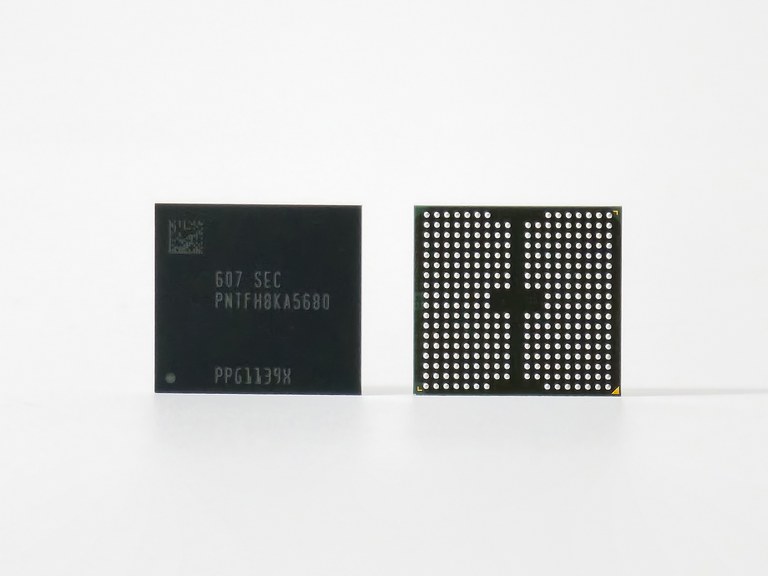
Samsung Electronics unveiled next-generation 3D memory architecture mockups for the first time, solidifying its technology strategy to address AI infrastructure demands. By presenting vertical integration structures that transcend the physical limitations of conventional stacking methods and ultra-high-layer NAND technology, the company demonstrated its memory technology competitiveness.
Samsung Electronics announced that it displayed mockups of next-generation 3D memory architecture zHBM and zNAND-O at 'FMS (Future of Memory and Storage) 2026' held at the Santa Clara Convention Center in California on August 4-6, with the unveiling on August 5.
Lee Jin-yeop, Vice President of the Flash Development Division, and Kim Gyeong-ryun, Executive Vice President of the DRAM Development Division, delivered keynote speeches introducing next-generation memory technology vision and AI infrastructure response roadmap.
zHBM is a next-generation architecture that vertically stacks HBM on top of AI accelerators (xPU), reducing data movement distance compared to the conventional method of placing HBM beside accelerators, thereby enhancing bandwidth and power efficiency.
According to Samsung Electronics, systems employing zHBM deliver up to 8x higher performance compared to HBM5, improve power efficiency by up to 3x, and reduce thermal resistance by over 50%.
By adding customized IP (Intellectual Property) to the interlayer, customer-tailored design is also possible, including memory capacity expansion and accelerator performance enhancement.
zNAND-O is a high-performance NAND solution that combines TSV (Through Silicon Via) with existing V-NAND vertical stacking technology to achieve 3D packaging of 4-tier or 8-tier chips.
Optimized for on-device AI environments, Samsung Electronics explained that the product supports real-time large-scale data processing based on high space efficiency and fast response speed.
At this event, Samsung Electronics also unveiled the 10th generation V-NAND 'V10 BV-NAND' featuring a vertical stacking structure of over 400 layers.
By applying wafer bonding technology and 3 Stack technology, the company increased memory integration density by approximately 58% compared to the previous generation (V9), and also improved data read/write performance and I/O speed.
Next-generation memory and storage portfolio was also showcased.
The company exhibited △HBM4E △HBM5 mockups △LPDDR5X-PIM △PM1763 △BM1773 and others.
In particular, Samsung Electronics introduced LPDDR5X-PIM as a product that performs computations within memory to reduce data movement and enhance power efficiency.
Samsung Electronics emphasized its 'one-stop solution' capability to provide integrated support from customer design stages to mass production based on its comprehensive semiconductor (IDM) system encompassing memory, logic, foundry, and packaging.

Comments
Related news
Samsung Electronics Establishes 'RX Business Promotion Office' Directly Under the CEO
Samsung Electronics has established the 'RX Business Promotion Office' reporting directly to the CEO to promote the integration of its robotics business. It is building a system that consolidates company-wide technologies and capabilities, handling everything from mid-to-long-term strategy to commercialization, with the Seoul R&D Campus serving as the main hub and overseas research centers in the United States, China, and Japan also operating. Vice President Lee Dong-gun, who led the Boston Dynamics strategy, has been appointed as the head of the Robotics Strategy Team, and external experts including professors from Seoul National University and Ajou University are also participating.
2026.07.21by 배종인 기자
Samsung Electronics Service Ranks 1st in KSQI Home Appliance & Mobile After-sales Service Sector
Samsung Electronics Service has ranked first for 16 consecutive years in home appliance after-sales service and 15 consecutive years in mobile and IT device after-sales service on the Korean Industry Service Quality Index (KSQI). This year, the company expanded reservation services to all service centers nationwide and extended available reservation days through Saturday mornings, resulting in more than double the number of customers using the service in June compared to March. Service accessibility has been improved through SmartThings connected services, Plus inspection, and on-site support for remote and rural areas.
2026.07.22by 명세환 기자
Samsung Electronics and Broadcom Sign $200 Billion MOU Over 5 Years
Samsung Electronics and Broadcom are pursuing strategic cooperation worth a total of $200 billion through 2030. In response to the expansion of AI infrastructure, the two companies will collaborate across all sectors of AI semiconductors, from supplying advanced memory such as HBM4 and HBM4E to foundry services for sub-2nm processes and next-generation packaging technologies.
2026.07.26by 배종인 기자
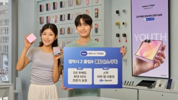
Samsung Electronics Revamps 'New Galaxy AI Subscription Club'... New 3-Year and Youth Benefits Introduced
Samsung Electronics has completely redesigned its 'New Galaxy AI Subscription Club' in line with the launch of the Galaxy Z Fold8 and Flip8. Key features include the new 'Flip Youth Subscription' targeting consumers in their 10s and 20s, the addition of a 3-year membership option, a guarantee of up to 50% residual value upon device return, and compensation of up to 3 million won for cyber financial damages. The company is offering differentiated subscription benefits that reflect customer lifestyle and financial security.
2026.07.26by 명세환 기자
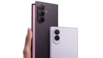
Samsung Electronics Begins Pre-sales for Galaxy Z Fold 8 Ultra, Flip 8, and Watch 9
Samsung Electronics will begin pre-orders for the Galaxy Z Fold8 Ultra and Fold8, Z Flip8, Watch Ultra2, and Watch9 from the 28th through August 3rd. The company is launching the eighth-generation foldable phone lineup and new smartwatches simultaneously, offering customers who purchase the 256GB model a complimentary storage upgrade to 512GB as a double storage benefit. The company is also providing various other benefits including up to 50% residual value compensation when devices are returned after one year upon enrollment in the Galaxy AI Subscription Club.
2026.07.27by 명세환 기자











